CX11250 Ver la hoja de datos (PDF) - Unspecified
Número de pieza
componentes Descripción
Fabricante
CX11250 Datasheet PDF : 62 Pages
| |||
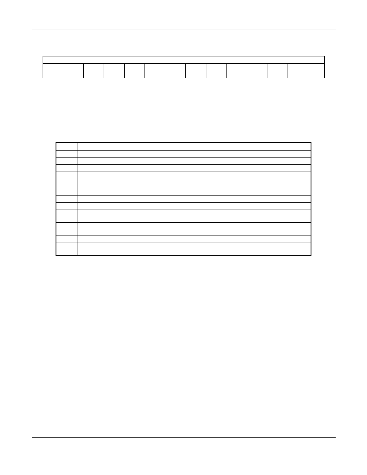
4.1.4 0x06 - Status Register
SmartHSF Mobile Modem Data Sheet
15
14
13
12
11
r/c
r/c
r/c
r/c
r/c
Status Register Bits
10 – 9
8
7
6
5
4
01
r/c
0
0
0
1
3-0
0000
r/c indicates the bit is readable and clearable (by writing a ‘1’ to corresponding bit position)
The Status Register bits are described in Table 4-3.
Status register bits may be cleared by writing a ‘1’ in the bit position corresponding to the bit position to be cleared. It is not
possible to set a status register bit by writing from the PCI Bus. Writing a ‘0’ has no effect in any bit position.
Bit
3-0
4
7-5
8
10-9
11
12
13
14
15
Table 4-3. Status Register
Description
Reserved
Extended capabilities = 1.
Not Implemented.
This bit is only implemented by bus masters. It is set when three conditions are met: 1) the bus agent
asserted PERR# itself or observed PERR# asserted; 2) the agent setting the bit acted as the bus master
for the operation in which the error occurred; and 3) the Parity Error Response bit (Command Register) is
set.
These bits encode the timing of DEVSEL#. 01 is supported corresponding to medium speed.
Signaled Target Abort. Not implemented.
Received Target Abort. This bit must be set by a master device whenever its transaction is terminated with
Target-Abort.
Received Master Abort. This bit must be set by a master device whenever its transaction (except for
Special Cycle) is terminated with Master-Abort.
Signaled System Error. This bit must be set whenever the device asserts SERR#.
Detected Parity Error. This bit must be set by the device whenever it detects a parity error, even if parity
error handling is disabled (as controlled by bit 6 in the Command register).
4.1.5 0x08 - Revision ID Field
This 8-bit read-only field identifying the device revision number is hardcoded in the device.
4.1.6 0x09 - Class Code Field
This 24-bit field, contains three 8-bit sub-fields. The upper byte is a base class code: 07 indicates a communications
controller. The middle byte is a sub-class code: 80 indicates “other” type of device. The lower byte is 00 which indicates no
register level programming defined. The value of the entire Class Code field is 0x078000.
4.1.7 0x0D - Latency Timer Register
The Latency Timer register specifies, in units of PCI Bus clocks, the value of the Latency Timer for this PCI Bus master. This
register has 5 read/write bits (MSBs) plus 3 bits of hardwired zero (LSBs). The Latency Timer Register is loaded into the PCI
Latency counter each time FRAME# is asserted to determine how long the master is allowed to retain control of the PCI Bus.
This register is loaded by system software. The default value for Latency Timer is 00.
4.1.8 0x0E - Header Type Field
Hardwired to 00.
4.1.9 0x28 - CIS Pointer Register
This register points to the CIS memory located in the HSD’s memory space.
4.1.10 0x2C - Subsystem Vendor ID Register
Subsystem Vendor ID register is supported. Loaded from the serial EEPROM after PCIRST# is deasserted.
100553B
Conexant
4-3
Share Link: 