AD5721 Ver la hoja de datos (PDF) - Analog Devices
Número de pieza
componentes Descripción
Fabricante
AD5721 Datasheet PDF : 31 Pages
| |||
AD5761/AD5721
ABSOLUTE MAXIMUM RATINGS
TA = 25°C, unless otherwise noted. Transient currents of up to
200 mA do not cause silicon controlled rectifier (SCR) latch-up.
Table 5.
Parameter
VDD to AGND
VSS to AGND
VDD to VSS
DVCC to DGND
Digital Inputs1 to DGND
Digital Outputs2 to DGND
VREFIN to DGND
VOUT to AGND
AGND to DGND
Operating Temperature Range,
TA Industrial
Storage Temperature Range
Junction Temperature, TJ MAX
Thermal Impedance
16-Lead TSSOP
θJA
θJC
16-Lead LFCSP
θJA
θJC
Power Dissipation
Lead Temperature
Soldering
ESD (Human Body Model)
Rating
−0.3 V to +34 V
+0.3 V to −17 V
−0.3 V to +34 V
−0.3 V to +7 V
−0.3 V to DVCC + 0.3 V or 7 V
(whichever is less)
−0.3 V to DVCC + 0.3 V or 7 V
(whichever is less)
−0.3 V to +7 V
VSS to VDD
−0.3 V to +0.3 V
−40°C to +125°C
−65°C to +150°C
150°C
113°C/W3
28°C/W
75°C/W3
4.5°C/W4
(TJ MAX − TA)/θJA
JEDEC industry standard
J-STD-020
4 kV
1 The digital inputs include CLEAR, RESET, SCLK, SYNC, SDI, and LDAC.
2 The digital outputs include ALERT and SDO.
3 JEDEC 2S2P test board, still air (0 m/sec airflow).
4 Measured to exposed paddle, with infinite heat sink on package top surface.
Data Sheet
Stresses at or above those listed under Absolute Maximum
Ratings may cause permanent damage to the product. This is a
stress rating only; functional operation of the product at these
or any other conditions above those indicated in the operational
section of this specification is not implied. Operation beyond
the maximum operating conditions for extended periods may
affect product reliability.
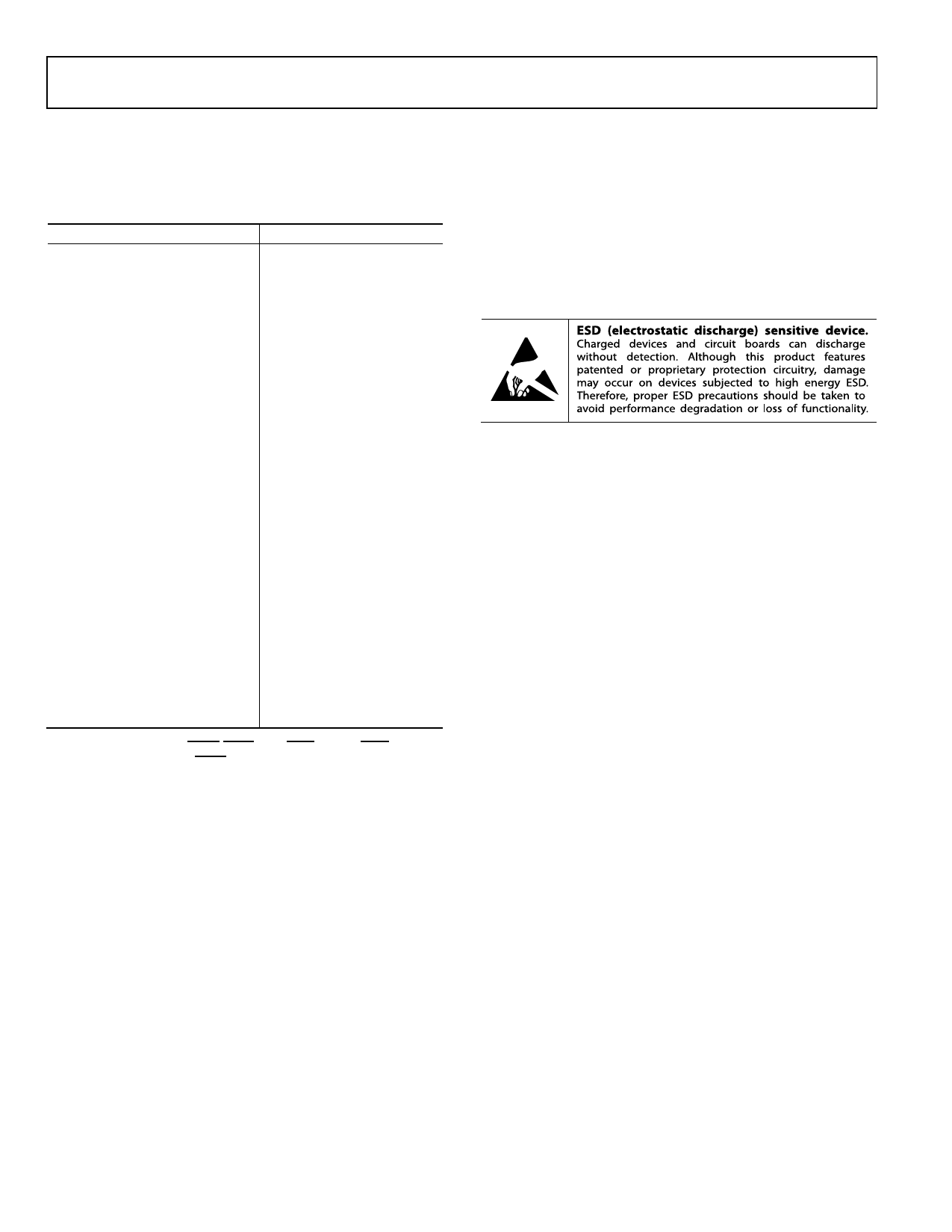
ESD CAUTION
Rev. C | Page 8 of 31
Share Link: 