MT90737AM Ver la hoja de datos (PDF) - Mitel Networks
Número de pieza
componentes Descripción
Fabricante
MT90737AM Datasheet PDF : 40 Pages
| |||
MT90737 CMOS
Preliminary Information
DS3 Interface
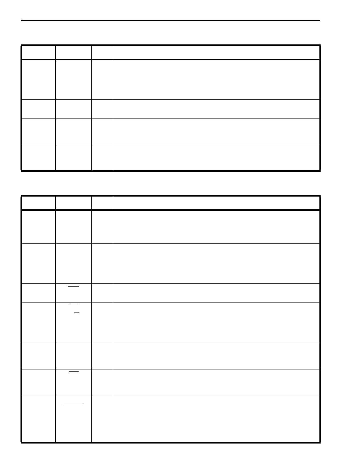
Pin #
Name I/O/P
Description
68
DS3CR
I DS3 Receive Clock. CMOS compatible. A 44.736 MHz clock that is used to
clock DS3 data into the MT90737. This clock is used as the time base for
demultiplexing the DS3 data. When the loop timing feature is active (a one
written into bit 3 (LPTIME) in 02H), or when the DS3 external transmit clock
(XCK) fails, DS3CR becomes the transmit clock.
69
DS3DR
I DS3 Receive Data. CMOS compatible. Receive 44.736 Mbit/s data is clocked
into the MT90737 on positive transitions of the receive clock (DS3CR).
125
DS3CT
O DS3 Transmit Clock. TTL Type IV compatible. A 44.736 MHz clock which is
derived from the external transmit clock input signal (XCK). It is used to clock
DS3 data from the MT90737.
93
DS3DT
O DS3 Transmit Data. TTL Type IV compatible. Transmit C-bit parity or M13 for-
matted DS3 data is clocked out of the MT90737 on positive transitions of the
transmit clock (DS3CT).
Note: I = Input; O = Output; P = Power. See DC Characteristics section for CMOS and TTL Type definitions.
Microprocessor Interface
Pin #
Name I/O/P
Description
60-57
48-45
76-83
74
71
73
72
163
A(7-4)
A(3-0)
A/D (7-0)
D(7-0)
SEL
RD
R/W
ALE
WR
RDY
DTACK
I Address Bus (Intel/Motorola). TTL Type II compatible. These are active high
address inputs that are used by the microprocessor for accessing the
MT90737 registers for a read/write operation. A7 is the most significant bit.
These signals are ignored when the multiplexed interface is selected.
I/O Address/Data Bus (Multiplexed), Data Bus (Intel/Motorola). TTL Type IV
compatible. For a multiplexed interface, these bi-directional leads constitute
address/data buses for accessing the MT90737 registers. For either the Intel
or Motorola interface, these bi-directional leads are used for transferring data.
The most significant bit is A/D7 or D7.
I Select. TTL Type I compatible. A low enables data transfers between the
microprocessor and the MT90737 registers during a read/write bus cycle.
I Read (Intel/Multiplexed) or Read/Write (Motorola). TTL Type I compatible.
Intel/Multiplexed - An active low signal generated by the microprocessor for
reading the MT90737 register locations. Motorola - An active high signal gen-
erated by the microprocessor for reading the MT90737 register locations. An
active low signal is used to write to the MT90737 register locations.
I Address Latch Enable (Multiplexed). TTL Type I compatible. An active high
enable signal generated by the microprocessor. The falling transition is used to
store an address during a read/write bus cycle.
I Write (Intel/Multiplexed). TTL Type I compatible. An active low signal gener-
ated by the Intel/Multiplexed microprocessor for writing to the MT90737 regis-
ter locations. Not used for the Motorola microprocessor interface.
O Ready (Intel) or Data Transfer Acknowledge (Motorola Mode). TTL Type IV
compatible. Intel - The MT90737 is always Ready. Connection to an Intel
Microprocessor is optional. If connected, a pull-up resistor is required. Motor-
ola - During a read cycle, a low signal indicates the information on the data bus
is valid. During a write cycle, a low signal acknowledges the acceptance of
data. A pull-up resistor is required for this pin.
5-68
Share Link: 