WM8602 Ver la hoja de datos (PDF) - Wolfson Microelectronics plc
Número de pieza
componentes Descripción
Fabricante
WM8602 Datasheet PDF : 46 Pages
| |||
WM8602
Product Preview
SIGNAL TIMING REQUIREMENTS
POWER SUPPLY
Test Conditions
AGND, DGND, BGDN = 0V, TA = +25°C
PARAMETER
Power Supply Timing Information
AVDD: rise time 10% to 90% AVDD
DVDD: rise time 10% to 90% DVDD
BVDD: rise time 10% to 90% BVDD
Table 2 Power Supply Timing Requirements
SYMBOL
tAR
tDR
tBR
MIN
0.2
0.2
0.2
TYP
MAX
50
50
50
UNIT
ms
ms
ms
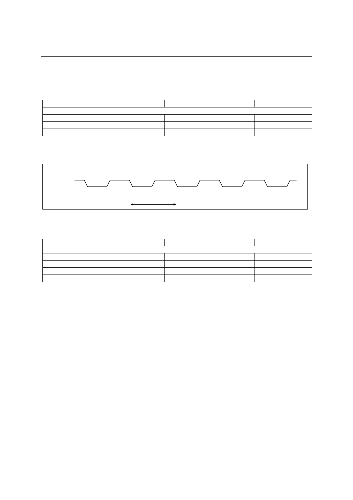
MASTER CLOCK TIMING
XTI/MCLK
tMCLKY
Figure 1 Master Clock Timing Requirements
Test Conditions
AVDD, DVDD, BVDD = 3.3V, AGND, DGND, BGDN = 0V, TA = +25°C
PARAMETER
SYMBOL
System Clock Timing Information
XTI/MCLK System clock cycle time
tMCLKY
XTI/MCLK Duty cycle
XTI/MCLK Period Jitter
XTI/MCLK Rise/Fall times 10% to 90% AVDD
Table 3 Master Clock Timing Requirements
MIN
20
40:60
TYP
MAX
100
60:40
200
3
UNIT
ns
%
ps
ns
w
PP Rev 1.5 May 2004
8
Share Link: 