MJF6388(2002) Ver la hoja de datos (PDF) - ON Semiconductor
Número de pieza
componentes Descripción
Fabricante
MJF6388 Datasheet PDF : 8 Pages
| |||
ON Semiconductor)
Complementary Power
Darlingtons
For Isolated Package Applications
NPN
MJF6388 *
PNP
MJF6668 *
*ON Semiconductor Preferred Devices
Designed for general–purpose amplifiers and switching
applications, where the mounting surface of the device is required to
be electrically isolated from the heatsink or chassis.
• Isolated Overmold Package, TO–220 Type
• Electrically Similar to the Popular 2N6388, 2N6668, TIP102 and
TIP107
• 100 VCEO(sus)
• 10 A Rated Collector Current
• No Isolating Washers Required
• Reduced System Cost
• High DC Current Gain — 1000 (Min) @ IC = 5.0 Adc
• High Isolation Voltage (up to 4500 VRMS)
• Case 221D is UL Recognized at 3500 VRMS: File #E69369
COMPLEMENTARY
SILICON
POWER DARLINGTONS
10 AMPERES
100 VOLTS
40 WATTS
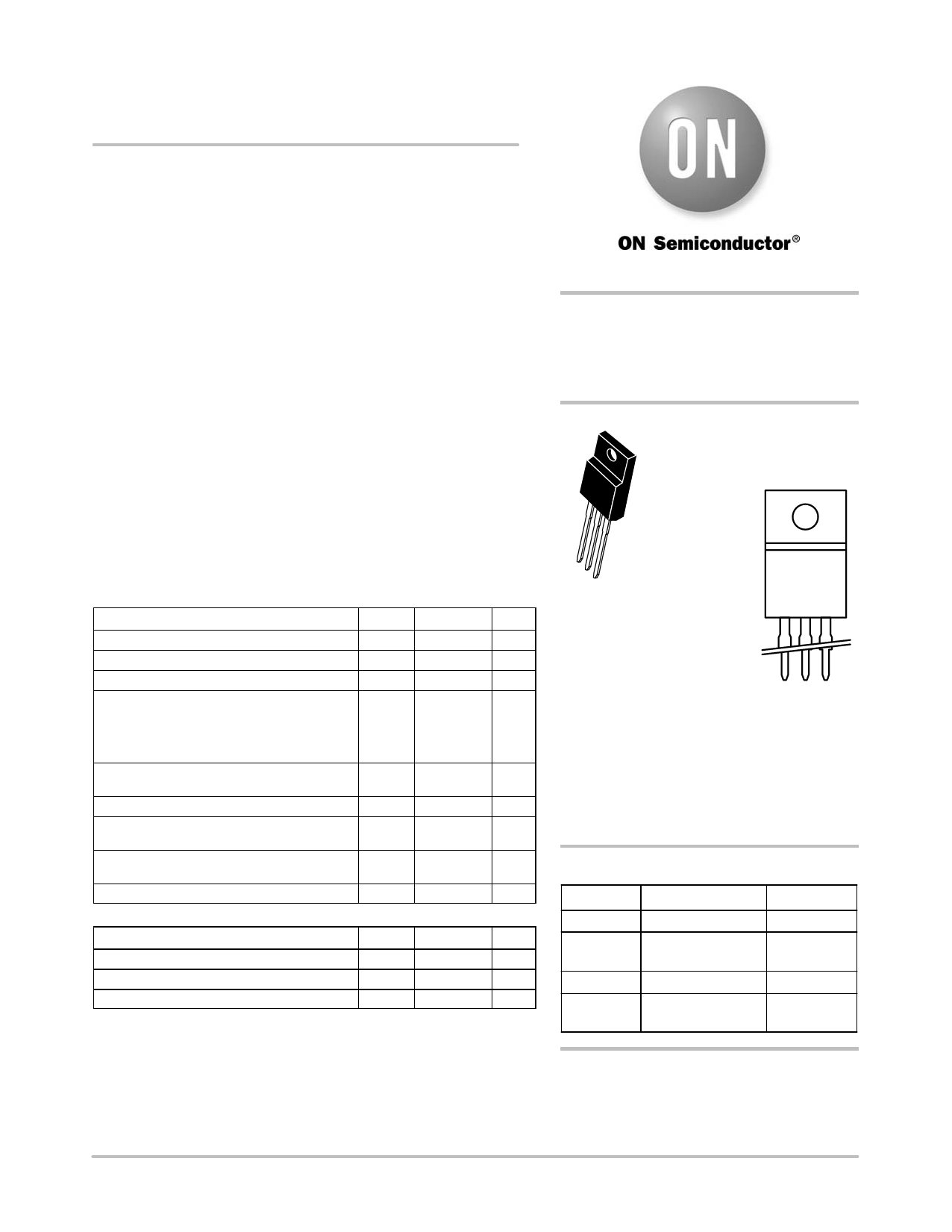
1
2
STYLE 2:
3
PIN 1. BASE
2. COLLECTOR
3. EMITTER
ÎÎÎÎÎÎÎÎÎÎÎÎÎÎÎÎÎÎÎÎÎÎÎÎÎÎÎÎÎÎÎÎÎ MAXIMUM RATINGS
ÎÎÎÎÎÎÎÎÎÎÎÎÎÎÎÎÎÎÎÎÎÎÎÎÎÎÎÎÎÎÎÎÎ Collector–Emitter Voltage
Rating
ÎÎÎÎÎÎÎÎÎÎÎÎÎÎÎÎÎÎÎÎÎÎÎÎÎÎÎÎÎÎÎÎÎ Collector–Base Voltage
ÎÎÎÎÎÎÎÎÎÎÎÎÎÎÎÎÎÎÎÎÎÎÎÎÎÎÎÎÎÎÎÎÎ Emitter–Base Voltage
ÎÎÎÎÎÎÎÎÎÎÎÎÎÎÎÎÎÎÎÎÎÎÎÎÎÎÎÎÎÎÎÎÎ RMS Isolation Voltage (1)
ÎÎÎÎÎÎÎÎÎÎÎÎÎÎÎÎÎÎÎÎÎÎÎÎÎÎÎÎÎÎÎÎÎ (for 1 sec, R.H. < 30%, TA = 25_C)
ÎÎÎÎÎÎÎÎÎÎÎÎÎÎÎÎÎÎÎÎÎÎÎÎÎÎÎÎÎÎÎÎÎÎÎÎÎÎÎÎÎÎÎÎÎÎÎÎÎÎÎÎÎÎÎÎÎÎÎÎÎÎÎÎÎÎ CollectorCurrent — Continuous
— Peak(2)
ÎÎÎÎÎÎÎÎÎÎÎÎÎÎÎÎÎÎÎÎÎÎÎÎÎÎÎÎÎÎÎÎÎ Base Current
ÎÎÎÎÎÎÎÎÎÎÎÎÎÎÎÎÎÎÎÎÎÎÎÎÎÎÎÎÎÎÎÎÎÎÎÎÎÎÎÎÎÎÎÎÎÎÎÎÎÎÎÎÎÎÎÎÎÎÎÎÎÎÎÎÎÎ Total Power Dissipation* @ TC = 25_C
Derate above 25_C
ÎÎÎÎÎÎÎÎÎÎÎÎÎÎÎÎÎÎÎÎÎÎÎÎÎÎÎÎÎÎÎÎÎ Total Power Dissipation @ TA = 25_C
ÎÎÎÎÎÎÎÎÎÎÎÎÎÎÎÎÎÎÎÎÎÎÎÎÎÎÎÎÎÎÎÎÎ Derate above 25_C
ÎÎÎÎÎÎÎÎÎÎÎÎÎÎÎÎÎÎÎÎÎÎÎÎÎÎÎÎÎÎÎÎÎ Operating and Storage Junction Temperature Range
ÎÎÎÎÎÎÎÎÎÎÎÎÎÎÎÎÎÎÎÎÎÎÎÎÎÎÎÎÎÎÎÎÎ THERMAL CHARACTERISTICS
ÎÎÎÎÎÎÎÎÎÎÎÎÎÎÎÎÎÎÎÎÎÎÎÎÎÎÎÎÎÎÎÎÎ Characteristic
ÎÎÎÎÎÎÎÎÎÎÎÎÎÎÎÎÎÎÎÎÎÎÎÎÎÎÎÎÎÎÎÎÎ Thermal Resistance, Junction to Case*
ÎÎÎÎÎÎÎÎÎÎÎÎÎÎÎÎÎÎÎÎÎÎÎÎÎÎÎÎÎÎÎÎÎ Thermal Resistance, Junction to Ambient
ÎÎÎÎÎÎÎÎÎÎÎÎÎÎÎÎÎÎÎÎÎÎÎÎÎÎÎÎÎÎÎÎÎ Lead Temperature for Soldering Purpose
ÎÎÎÎÎÎÎÎÎÎÎÎÎÎÎÎÎÎÎÎÎÎÎÎÎÎÎÎÎÎÎÎÎ (1) Proper strike and creepage distance must be provided.
Test No. 1 Per Figure 14
Test No. 2 Per Figure 15
Test No. 3 Per Figure 16
Symbol
VCEO
VCB
VEB
VISOL
IC
IB
PD
PD
TJ, Tstg
Symbol
RθJC
RθJA
TL
CASE 221D–02
UL RECOGNIZED
Value
100
100
5.0
4500
3500
1500
10
15
1.0
40
0.31
2.0
0.016
–65 to +150
Unit
Vdc
Vdc
Vdc
V
Adc
Adc
Watts
W/_C
Watts
W/_C
_C
Max
Unit
3.2
_C/W
62.5
_C/W
260
_C
(2) Pulse Test: Pulse Width = 5.0 ms, Duty Cycle v 10%.
*Measurement made with thermocouple contacting the bottom insulated mounting surface of the package (in a location beneath the die), the
device mounted on a heatsink, thermal grease applied and a mounting torque of 6 to 8 inSlbs.
Preferred devices are ON Semiconductor recommended choices for future use and best overall value.
© Semiconductor Components Industries, LLC, 2002
1
April, 2002 – Rev. 6
Publication Order Number:
MJF6388/D
Share Link: 