M80C186 Ver la hoja de datos (PDF) - Intel
Número de pieza
componentes Descripción
Fabricante
M80C186 Datasheet PDF : 59 Pages
| |||
M80C186
Timer Operation
The timers are controlled by 11 16-bit registers in
the internal peripheral control block The configura-
tion of these registers is shown in Table 15 The
count register contains the current value of the tim-
er It can be read or written at any time independent
of whether the timer is running or not The value of
this register will be incremented for each timer
event Each of the timers is equipped with a MAX
COUNT register which defines the maximum count
the timer will reach After reaching the MAX COUNT
register value the timer count value will reset to zero
during that same clock i e the maximum count val-
ue is never stored in the count register itself Timers
0 and 1 are in addition equipped with a second
MAX COUNT register which enables the timers to
alternate their count between two different MAX
COUNT values programmed by the user If a single
MAX COUNT register is used the timer output pin
will switch LOW for a single clock 1 clock after the
maximum count value has been reached In the dual
MAX COUNT register mode the output pin will indi-
cate which MAX COUNT register is currently in use
thus allowing nearly complete freedom in selecting
waveform duty cycles For the timers with two MAX
COUNT registers the RIU bit in the control register
determines which is used for the comparison
Each timer gets serviced every fourth CPU-clock cy-
cle and thus can operate at speeds up to one-quar-
ter the internal clock frequency (one-eighth the crys-
tal rate) External clocking of the timers may be done
at up to a rate of one-quarter of the internal CPU-
clock rate Due to internal synchronization and pipe-
lining of the timer circuitry a timer output may take
up to 6 clocks to respond to any individual clock or
gate input
Since the count registers and the maximum count
registers are all 16 bits wide 16 bits of resolution are
provided Any Read or Write access to the timers will
add one wait state to the minimum four-clock bus
cycle however This is needed to synchronize and
coordinate the internal data flows between the inter-
nal timers and the internal bus
The timers have several programmable options
All three timers can be set to halt or continue on
a terminal count
Timers 0 and 1 can select between internal and
external clocks alternate between MAX COUNT
registers and be set to retrigger on external
events
The timers may be programmed to cause an in-
terrupt on terminal count
These options are selectable via the timer mode
control word
Timer Mode Control Register
The mode control register (see Figure 20) allows
the user to program the specific mode of operation
or check the current programmed status for any of
the three integrated timers
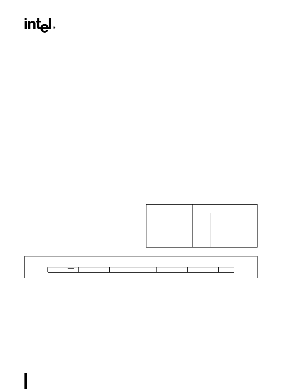
Table 15 Timer Control Block Format
Register Name
Register Offset
Tmr 0 Tmr 1 Tmr 2
Mode Control Word 56H
Max Count B
54H
Max Count A
52H
Count Register
50H
5EH
66H
5CH not present
5AH
62H
58H
60H
15
14
13
12
11
EN
INH
INT
RIU
0
5
4
3
2
1
0
MC RTG
P
EXT ALT CONT
Figure 20 Timer Mode Control Register
29
Share Link: 