TC2014 Ver la hoja de datos (PDF) - Microchip Technology
Número de pieza
componentes Descripción
Fabricante
TC2014 Datasheet PDF : 20 Pages
| |||
TC2014/2015/2185
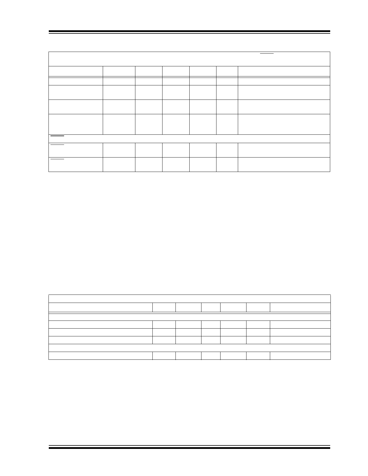
ELECTRICAL CHARACTERISTICS (CONTINUED)
Electrical Specifications: Unless otherwise specified, VIN = VR + 1V, IL = 100 µA, COUT = 3.3 µF, SHDN > VIH, TA = +25°C.
BOLDFACE type specifications apply for junction temperature of -40°C to +125°C.
Parameters
Sym
Min
Typ
Max
Units
Conditions
Thermal Regulation
VOUT/PD
—
Thermal Shutdown Die
TSD
—
Temperature
0.04
160
—
V/W Note 6, Note 7
—
°C
Output Noise
eN
—
200
—
nV/Hz IL = IOUTMAX, F = 10 kHz
470 pF from Bypass to GND
Response Time
TR
(from Shutdown Mode)
(Note 8)
—
60
—
µs VIN = 4V, IL = 30 mA,
CIN = 1 µF, COUT = 10 µF
SHDN Input
SHDN Input High
Threshold
VIH
60
—
—
%VIN VIN = 2.5V to 6.0V
SHDN Input Low
Threshold
VIL
—
—
15
%VIN VIN = 2.5V to 6.0V
Note 1: The minimum VIN has to meet two conditions: VIN = 2.7V and VIN = VR + VDROPOUT.
2: VR is the regulator output voltage setting. For example: VR = 1.8V, 2.7V, 2.8V, 2.85V, 3.0V, 3.3V.
3:
TCVOUT = ---V----O---U----T---M----A---X-V---–-O----UV---T-O---U----T---M--T--I--N-----------1---0----–---6-
4: Regulation is measured at a constant junction temperature using low duty cycle pulse testing. Load regulation is tested
over a load range from 1.0 mA to the maximum specified output current. Changes in output voltage due to heating
effects are covered by the Thermal Regulation specification.
5: Dropout Voltage is defined as the input-to-output differential at which the output voltage drops 2% below its nominal
value.
6: Thermal Regulation is defined as the change in output voltage at a time T after a change in power dissipation is applied,
excluding load or line regulation effects. Specifications are for a current pulse equal to IMAX at VIN = 6V for T = 10 ms.
7: The maximum allowable power dissipation is a function of ambient temperature, the maximum allowable junction
temperature and the thermal resistance from junction-to-air (i.e. TA, TJ, JA).
8: Time required for VOUT to reach 95% of VR (output voltage setting), after VSHDN is switched from 0 to VIN.
TEMPERATURE CHARACTERISTICS
Electrical Specifications: Unless otherwise noted, VDD = +2.7V to +6.0V and VSS = GND.
Parameters
Sym
Min
Typ
Max
Temperature Ranges:
Extended Temperature Range
Operating Temperature Range
Storage Temperature Range
Thermal Package Resistances:
Thermal Resistance, 5L-SOT-23
TA
-40
—
+125
TA
-40
—
+125
TA
-65
—
+150
JA
—
255
—
Units
°C
°C
°C
°C/W
Conditions
2001-2012 Microchip Technology Inc.
DS21662F-page 3
Share Link: 