ST7573 Ver la hoja de datos (PDF) - Sitronix Technology Co., Ltd.
Número de pieza
componentes Descripción
Fabricante
ST7573 Datasheet PDF : 46 Pages
| |||
ST7573
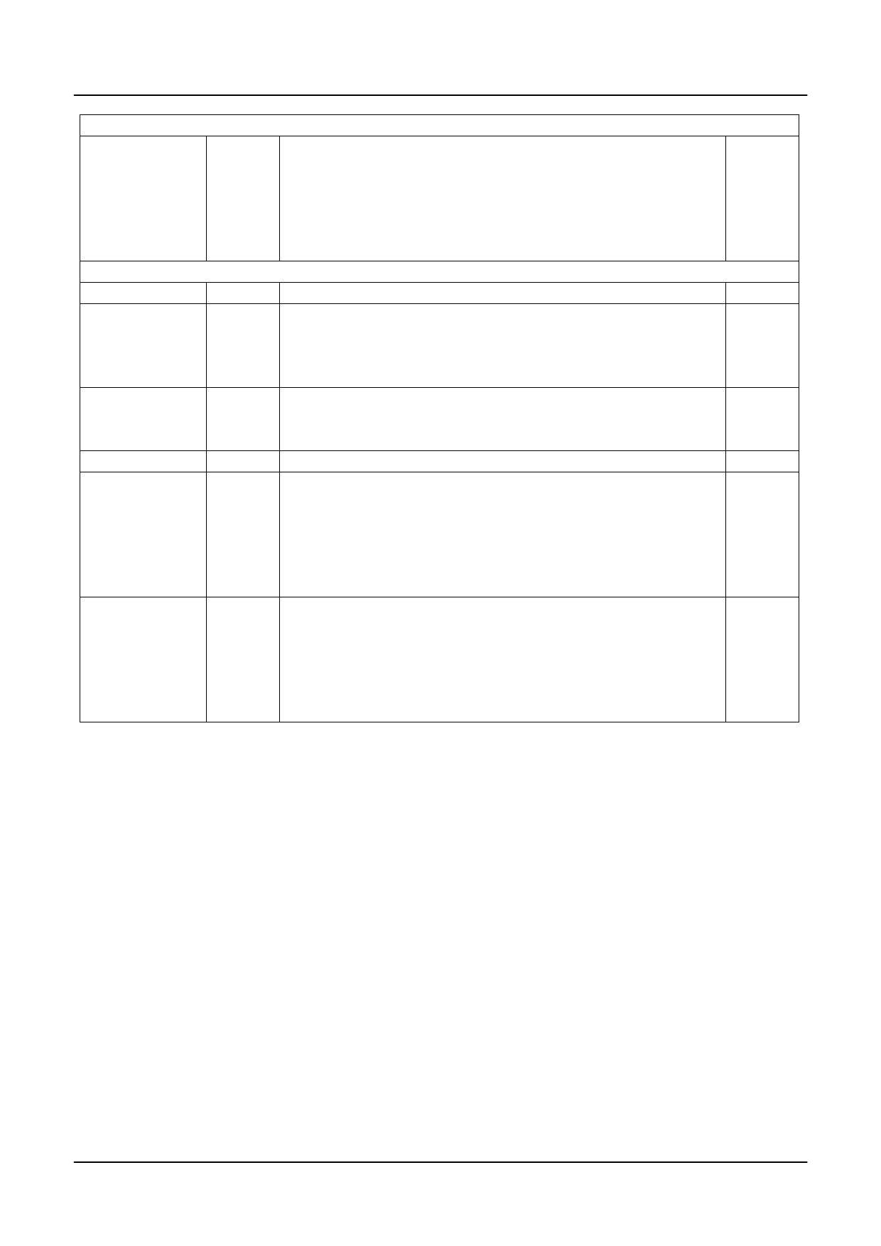
LCD DRIVER CLOCK SUPPLY
When the on-chip oscillator is used, this input must be connected to
OSC
VDD. An external clock signal, if used, is connected to this pin. The
oscillator and external clock are both inhibited by connecting the OSC pin
I
1
to VSS and the display is not clocked and may be left in a DC state. To
avoid this, the chip should always be put into Power Down Mode before
stopping the clock.
POWER SUPPLY PIN
VSS
Power Ground.
3
Digital Supply voltage.
VDD
Power The 2 supply rails, VDD and VDD2 , could be connected together (for single
10
power).
If a Digital Option pin is high, must be this level.
Analog Supply voltage.
VDD2
Power The 2 supply rails, VDD and VDD2 , could be connected together (for single
9
power).
VRS
Power Reference voltage. Must be left open.
1
Positive LCD driving voltage for commons.
V0I is the V0 power source for the LCD driver. If using external V0, apply
the external power source on these pads.
V0I, V0O, V0S
Power
7
V0O is the internal V0 regulator output pad.
V0S is the feedback for the internal V0 voltage compensation circuit.
They should be separate in ITO and be connected together by FPC.
Negative LCD driving voltage for commons.
XV0I is the XV0 power source for the LCD driver. If using external XV0,
apply the external power source on these pads.
XV0I, XV0O,XV0S Power
7
XV0O is the internal XV0 regulator output pad.
XV0S is the feedback for the internal XV0 voltage compensation circuit.
They should be separate in ITO and be connected together by FPC.
Ver 1.0b
9/46
2007/07/12
Share Link: 