RT9201 Ver la hoja de datos (PDF) - Richtek Technology
Número de pieza
componentes Descripción
Fabricante
RT9201 Datasheet PDF : 13 Pages
| |||
RT9201
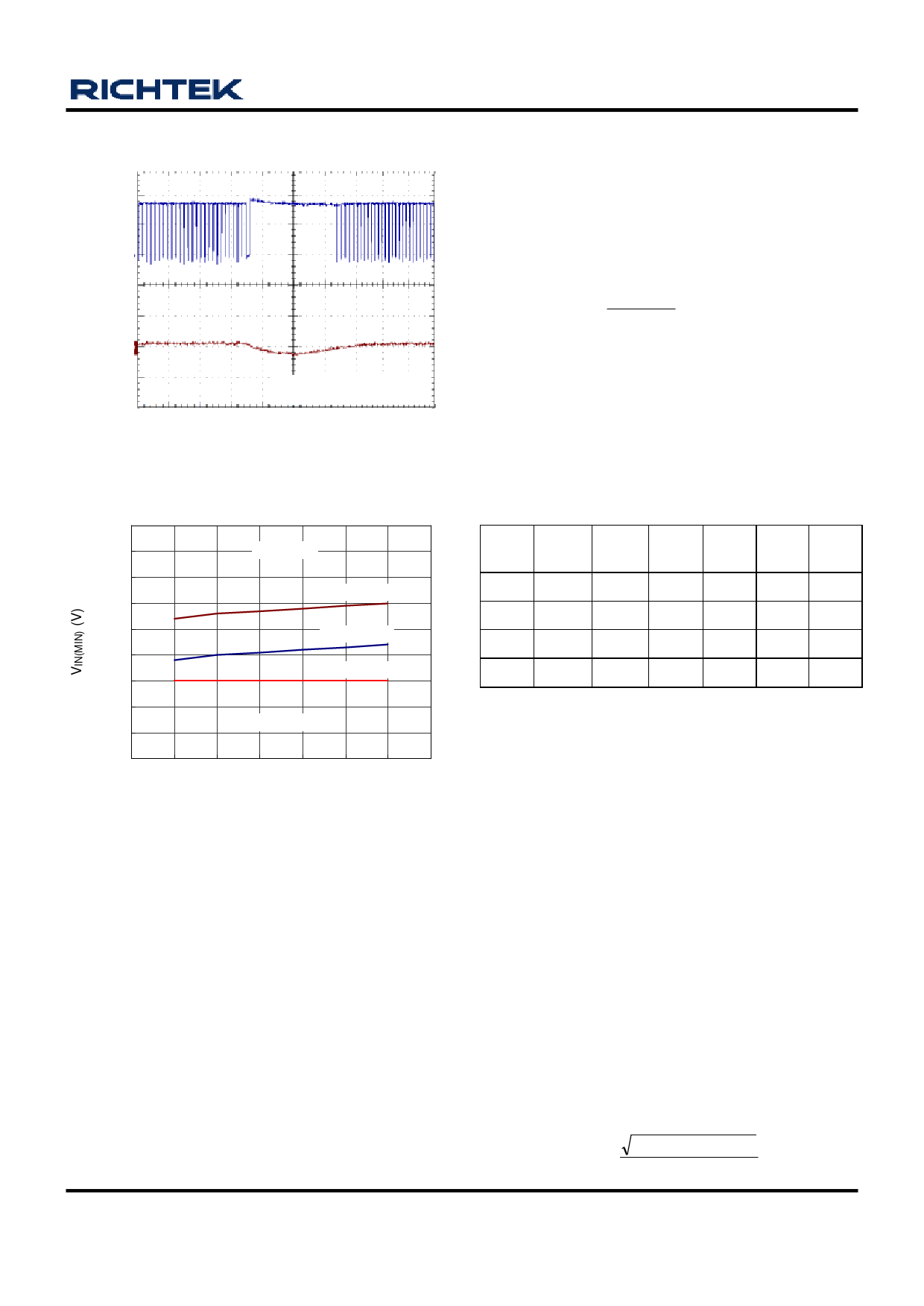
4
VLX 2
(V)
0
Sub-Harmonic at Boundary
Condition
100
VOUT
(mV) 0
-100
VIN = 3.8V, VOUT = 3.3V
IOUT = 600mA, COUT = 100uF
Time (10µs/Div)
Figure 1
BounMdina.ryInopfutPVWoMltaganedvsL.oOwu-tDpruotpCouurtreMnot de
5.50
5.00
PWM Mode
4.50
4.00
VOUT = 3.3V
3.50
3.00
2.50
VOUT = 2.5V
VOUT = 1.8V
2.00
Low Dropout Mode
1.50
1.00
0
100 200 300 400 500 600 700
OutpuItOCUTur(rmenAt)(mA)
Figure 2
Over Current Protection
The RT9201 continuously monitors the inductor current
by sensing the voltage across the PMOSFET when it
turns on. When the inductor current is higher than current
limit threshold (1A typical), OCP activates and forces the
PMOSFET turning off to limit inductor current cycle by
cycle.
The current limit is set to 50% level of normal condition
when the output voltage is lower than its 50% normal
level. This can minimize the power loss and protect the
device when over current or output short circuit occurs.
Once output voltage drops below to its 50% normal level
DS9201-12 August 2007
due to over current or short circuit, it can build up only
when output current is lower 50% of normal current limit
threshold.
Output Voltage Setting and Feedback Network
The output voltage can be set from VREF to VIN by a voltage
divider as:
VOUT
=
VREF
×
RF1 + RF2
RF2
The internal VREF is 0.8V with 1% accuracy. In practical
application, keep RF2 = 390kΩ and CF2 = 10pF
respectively and choose appropriate RF1 and CF1
according to the required output voltage. Make sure that
the product of RF1 and CF1 is about 8200kΩ-pF. The
following table shows recommended feedback network
as well as inductor for some typical output voltages.
Table 1. Component Selection for Typical Application
VOUT RF1
(V) (Ω)
CF1 RF2 CF2 LX CSS
(pF) (Ω) (pF) (µH) (pF)
0.85 24k 330 390k 10 4.7 330
1.5 343k 22 390k 10 6.8 470
2.5 820k 10 390k 10 10 680
3.3 1.2M 5.6 390k 10 10 1000
Inductor Selection
The output inductor is suggested as the above table for
optimal performance. Make sure that the inductor will
not saturate over the operation conditions including
temperature range, input voltage range, and maximum
output current. If possible, choose an inductor with rated
current higher than 1A so that it will not saturate even
under circuit condition.
Input Capacitor Selection
The input capacitor can filter the input peak current and
noise at input voltage source. The capacitor with low ESR
(effective series resistance) provides the small drop
voltage to stabilize the input voltage during the transient
loading. For input capacitor selection, the ceramic
capacitors larger than 10µF is recommend. The capacitor
must conform to the RMS current requirement. The
maximum RMS ripple current is calculated as :
IRMS = IOUT(MAX)
VOUT (VIN − VOUT )
VIN
www.richtek.com
11
Share Link: 