HTG2150 Ver la hoja de datos (PDF) - Holtek Semiconductor
Número de pieza
componentes Descripción
Fabricante
HTG2150 Datasheet PDF : 38 Pages
| |||
HTG2150
must be placed in TBLP. The TBLH is read only and
cannot be restored. If the main routine and the ISR
(Interrupt Service Routine) both employ the table read
instruction, the contents of the TBLH in the main rou-
tine are likely to be changed by the table read instruc-
tion used in the ISR. Errors can occur. In other words,
using the table read instruction in the main routine and
the ISR simultaneously should be avoided. However,
if the table read instruction has to be applied in both
the main routine and the ISR, the interrupt is sup-
posed to be disabled prior to the table read instruction.
It will not be enabled until the TBLH has been backed
up. All table related instructions need two cycles to
complete the operation. These areas may function as
normal program memory depending upon the require-
ments.
Stack register - STACK
This is a special part of the memory which is used to
save the contents of the program counter (PC) only. The
stack is organized into eight levels and is neither part of
the data nor part of the program space, and is neither
readable nor writeable. The activated level is indexed by
the stack pointer (SP) and is neither readable nor
writeable. At a subroutine call or interrupt acknowledg-
ment, the contents of the program counter and ROM ad-
dress A13 bit latch Data are pushed onto the stack. At
the end of a subroutine or an interrupt routine, signaled
by a return instruction (RET or RETI), the program coun-
ter and ROM address A13 bit latch Data are restored to
its previous value from the stack. After a chip reset, the
SP will point to the top of the stack.
If the stack is full and a non-masked interrupt takes place,
the interrupt request flag will be recorded but the acknowl-
edgment will be inhibited. When the stack pointer is decre-
mented (by RET or RETI), the interrupt will be serviced.
This feature prevents stack overflow allowing the pro-
grammer to use the structure more easily. In a similar
case, if the stack is full and a CALL is subsequently exe-
cuted, stack overflow occurs and the first entry will be lost
(only the most recent eight return address are stored).
Data memory - RAM
· Bank 0 (BP4~BP0=00000)
The Bank 0 data memory includes special purpose
and general purpose memory. The special purpose
memory is addressed from 00H to 2FH, while general
purpose memory is addressed from 40H to FFH. All
data memory areas can handle arithmetic, logic, in-
crement, decrement and rotate operations directly.
Except for some dedicated bits, each bit in the data
memory can be set and reset by the SET [m].i and
CLR [m].i instructions, respectively. They are also indi-
rectly accessible through the memory pointer registers
(MP0;01H, MP1;03H).
· Bank 15 (BP4~BP0=01111B)
The range of RAM starts from 80H to A7H. On the
LCD, every bit stands for one dot. If the bit is ²1², the
light of the dot on the LCD will be turned on. If the bit is
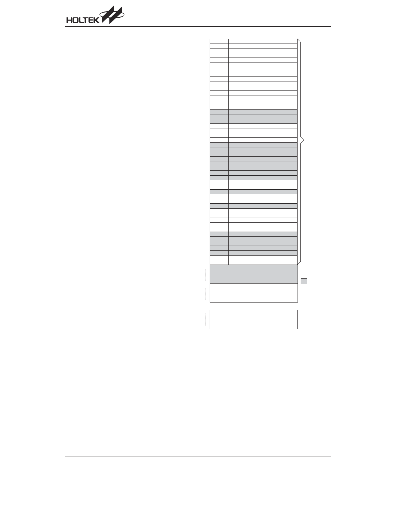
00H
IA R 0
01H
M P0
02H
IA R 1
03H
M P1
04H
BP
05H
ACC
06H
PCL
07H
TB LP
08H
TB LH
09H
W D TS
0A H STATU S
0B H
IN T C
0C H TM R 0H
0D H
TM R 0L
0E H TM R 0C
0.H
10H
11H
12H
PA
13H
PAC
14H
PB
15H
PBC
16H
17H
18H
19H
1A H
1B H
1C H
1D H
1 E H IN T C H
1.H
TBH P
20H
21H
TM R 2
22H TM R 2C
23H
24H
TM R 3
25H TM R 3C
2 6 H X 'T A L C
27H
PW M C
28H
PW M
29H
2A H
2B H
2C H
2D H
2E H
LC D C
2.H
COM R
30H
In d ir e c t A d d r e s s in g R e g is te r 0
M e m o r y P o in te r 0
In d ir e c t A d d r e s s in g R e g is te r 1
M e m o r y P o in te r 1
B a n k P o in te r
A c c u m u la to r
P r o g r a m C o u n te r L o w e r - b y te R e g is te r
T a b le P o in te r L o w e r - o r d e r B y te R e g is te r
T a b le H ig h e r - o r d e r B y te R e g is te r
W a tc h d o g T im e r O p tio n S e ttin g R e g is te r
S ta tu s R e g is te r
In te r r u p t C o n tr o l R e g is te r
T im e r C o u n te r 0 H ig h e r - o r d e r B y te R e g is te r
T im e r C o u n te r 0 L o w e r - o r d e r B y te R e g is te r
T im e r C o u n te r 0 C o n tr o l R e g is te r
P A I/O D a ta R e g is te r
P A I/O C o n tr o l R e g is te r
P B I/O D a ta R e g is te r
P B I/O C o n tr o l R e g is te r
In te r r u p t C o n tr o l H ig h e r - o r d e r B y te R e g is te r
T a b le P o in te r H ig h e r - o r d e r B y te R e g is te r
T im e r 2 R e g is te r
T im e r 2 C o n tr o l R e g is te r
T im e r 3 R e g is te r
T im e r 3 C o n tr o l R e g is te r
X 'ta l . a s t O s c illa to r u p C o n tr o l
P W M C o n tro l
P W M D a ta
L C D C o n tr o l R e g is te r
C o m m o n P a d A d d re s s R o ta to r
S p e c ia l P u r p o s e
D a ta M e m o ry
3.H
:U nused
40H
G e n e ra l P u rp o s e
R e a d a s "0 0 "
B a n k 0 D a ta M e m o ry
P B b it 3 /2 /1 /0 R e a d = 0
(1 9 2 B y te )
..H
80H
B a n k 1 5 D a ta M e m o ry
(4 0 B y te )
A 7H
RAM mapping
²0², then it will be turned off. Only MP1 can deal with
the memory of this range.
The contrast form of RAM location, COMMON, and
SEGMENT is as follows.
Indirect addressing register
Location 00H and 02H are indirect addressing registers
that are not physically implemented. Any read/write opera-
tion of [00H] and [02H] access data memory are pointed to
by MP0 (01H) and MP1 (03H) respectively. Reading loca-
tion 00H or 02H indirectly will return the result 00H. Writing
indirectly results in no operation.
Rev. 1.30
9
May 21, 2002
Share Link: 