NJU8721 Ver la hoja de datos (PDF) - Japan Radio Corporation
Número de pieza
componentes Descripción
Fabricante
NJU8721 Datasheet PDF : 13 Pages
| |||
NJU8721
! FUNCTIONAL DESCRIPTION
(1) Signal Output
PWM signals of L channel and R output from OUTL and OUTR terminals respectively. These signals are
converted to analog signal by external 2nd-order or over LC filter. The output driver power supplied from VDDL,
VDDR, VSSL, and VSSR are required high response power supply against voltage fluctuation like as switching
regulator because Output THD is effected by power supply stability.
(2) Master Clock
Master Clock is 256fS clock into MCK terminal for the internal circuit operation clock.
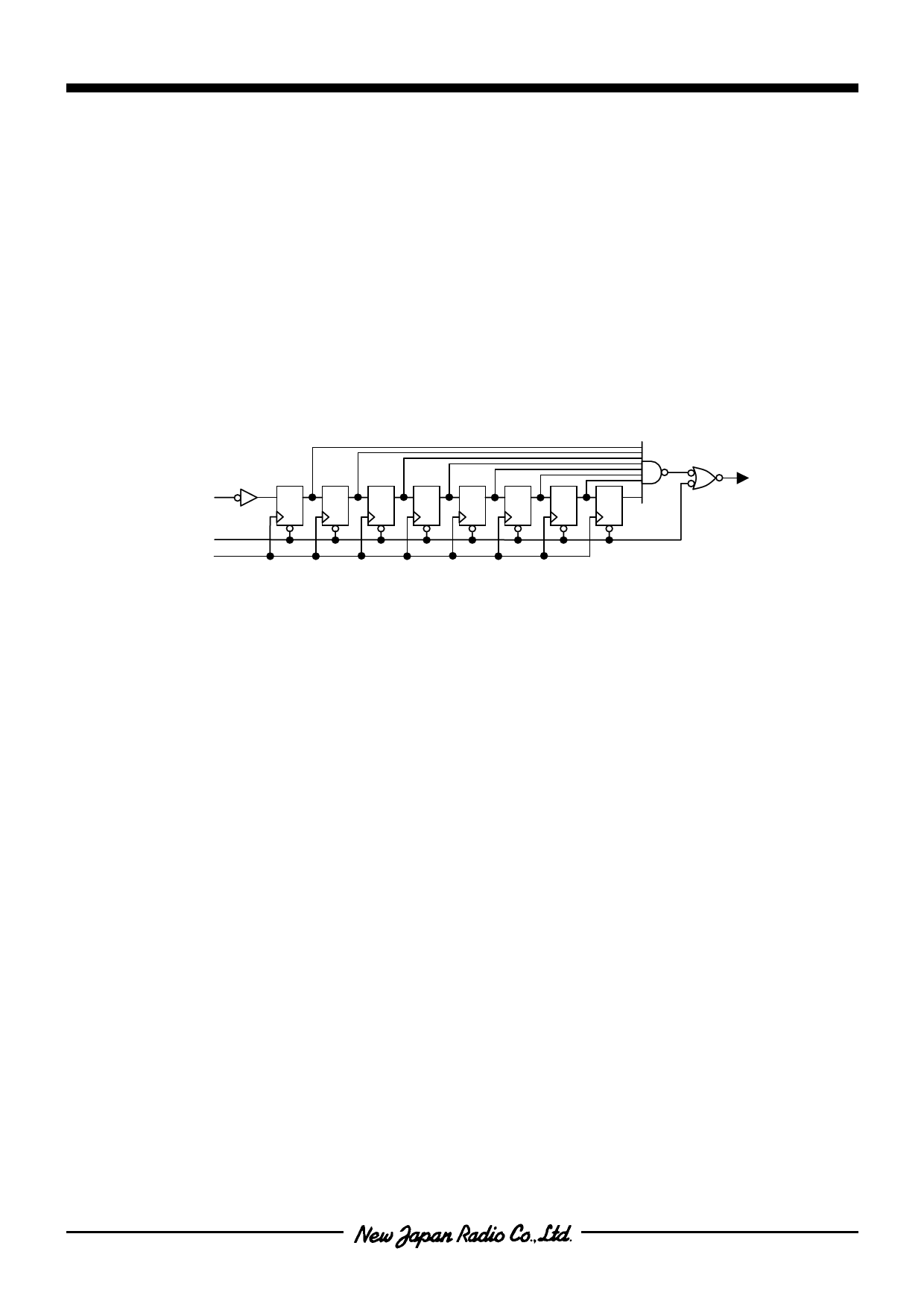
(3) Reset
“L” level input over than 3ms to the RST terminal is initialization signal to initialize the internal circuit. This
initialization signal is synchronized with internal clock and executes logical OR with the internal power on reset
signal. This Reset signal initializes the internal function setting registers also. During initialization, the
output-drivers output GND level. The reset equivalent circuit is shown bellow.
RST
Power on Reset
CLK
(About 10kHz)
D
D
D
D
D
D
D
D
Figure 1. Reset Equivalent Circuit
Internal Reset
(4) 8fS Over Sampling Digital Filter
8fS Over Sampling Digital Filter interpolates Audio data and decreases aliasing noise.
It realizes Attenuation and De-Emphasis function by serial function control.
(5) 32fS 6th ∆Σ & PWM
32fS 6th ∆Σ & PWM convert from Audio data of the 8fS Over Sampling Digital Filter to the 32fS one bit PWM
data.
-3-
Share Link: 