MC33298DWR2 Ver la hoja de datos (PDF) - Freescale Semiconductor
Número de pieza
componentes Descripción
Fabricante
MC33298DWR2 Datasheet PDF : 28 Pages
| |||
ELECTRICAL CHARACTERISTICS
MAXIMUM RATINGS
ELECTRICAL CHARACTERISTICS
MAXIMUM RATINGS
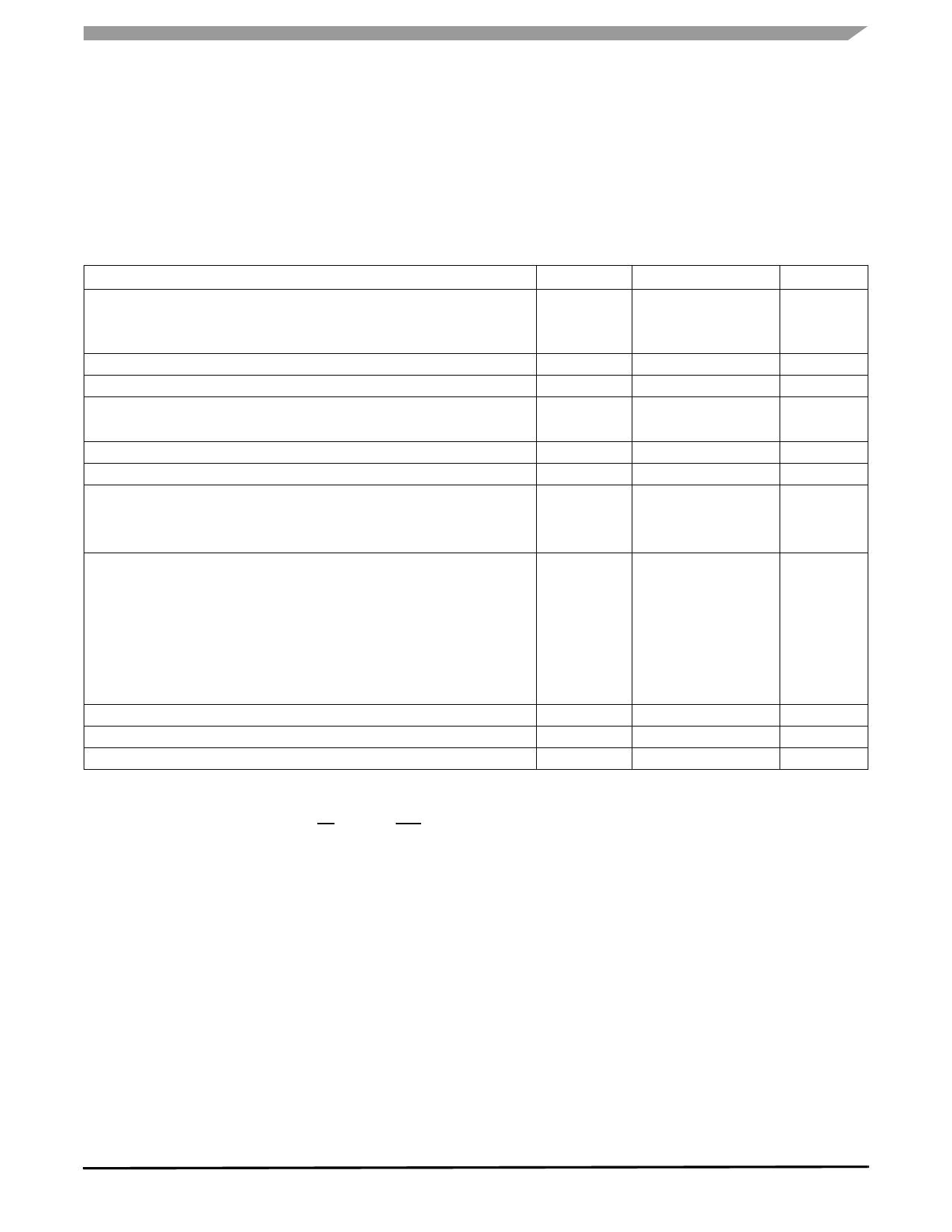
Table 3. Maximum Ratings
All voltages are with respect to ground unless otherwise noted. Exceeding these ratings may cause a malfunction or
permanent damage to the device.
Rating
Symbol
Value
Unit
Power Supply Voltage
Normal Operation (Steady-state)
Transient Conditions(1)
Logic Supply Voltage(2)
Input pin Voltage(3)
Output Clamp Voltage(4)
2.0mA ≤ IOUT ≤ 0.5A
V
VPWR(SS)
VPWR(PK)
- 1.5 to 26.5
- 13 to 60
VDD
- 0.3 to 7.0
V
VIN
- 0.3 to 7.0
V
VOUT(OFF)
V
50 to 75
Output Self-Limit Current
Continuous Per Output Current(5)
ESD Voltage(6)
Human Body Model(7)
Machine Model(7)
Output Clamp Energy(8)
Repetitive:
TJ = 25°C
TJ = 124°C
Non-Repetitive:
TJ = 25°C
TJ = 124°C
Recommended Frequency of SPI Operation(9)
Storage Temperature
Peak Package Reflow Temperature During Reflow(10),(11)
IOUT(LIM)
IOUT(CONT)
VESD1
VESD2
ECLAMP
fSPI
TSTG
TPPRT
3.0 to 6.0
1.0
2000
200
100
30
2.0
0.5
2.0
- 55 to 150
Note 11.
A
A
V
mJ
mJ
J
J
MHz
°C
°C
Notes
1. Transient capability with external 100Ω resistor in series with VP pin and supply.
2. Exceeding these limits may cause a malfunction or permanent damage to the device.
3. Exceeding the limits on SCLK, SI, CS, SFPD, or RST pins may cause permanent damage to the device.
4. With output OFF.
5. Continuous output current rating so long as maximum junction temperature is not exceeded. Operation at 125°C ambient temperature
will require maximum output current computation using package RθJA.
6. ESD data available upon request.
7. ESD1 testing is performed in accordance with the Human Body Model (CZap = 200pF, RZap = 1500Ω), ESD2 testing is performed in
accordance with the Machine Model (CZap = 200pF, RZap = 0Ω).
8. Maximum output clamp energy capability at 150°C junction temperature using a single non-repetitive pulse method.
9. Guaranteed and production tested for 2.0MHz SPI operation, but demonstrated to operate to 8.5MHz at 25°C.
10. Pin soldering temperature limit is for 10 seconds maximum duration. Not designed for immersion soldering. Exceeding these limits may
cause malfunction or permanent damage to the device.
11. Freescale’s Package Reflow capability meets Pb-free requirements for JEDEC standard J-STD-020C. For Peak Package Reflow
Temperature and Moisture Sensitivity Levels (MSL), Go to www.freescale.com, search by part number [e.g. remove prefixes/suffixes
and enter the core ID to view all orderable parts. (i.e. MC33xxxD enter 33xxx), and review parametrics.
Analog Integrated Circuit Device Data
Freescale Semiconductor
33298
5
Share Link: 