MB90350E Ver la hoja de datos (PDF) - Fujitsu
Número de pieza
componentes Descripción
Fabricante
MB90350E Datasheet PDF : 92 Pages
| |||
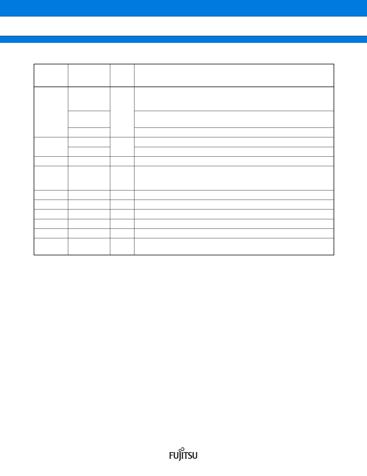
MB90350E Series
(Continued)
Pin No.
Pin name
I/O
Circuit
type*
Function
General purpose I/O port. The register can be set to select whether to use
P37
a pull-up resistor. This function is enabled either in single-chip mode or with
the CLK output disabled.
61
CLK
G CLK output pin. This function is enabled when both the external bus and
CLK output are enabled.
OUT7
Wave form output pin for output compare OCU7
62, 63
64
2
1
22, 23
P60, P61
AN0, AN1
AVCC
AVRH
AVSS
MD1, MD0
General purpose I/O ports
I
Analog input pins for A/D converter
K VCC power input pin for analog circuits
Reference voltage input for the A/D converter. This power supply must be
L turned on or off while a voltage higher than or equal to AVRH is applied to
AVCC.
K VSS power input pin for analog circuits
C Input pins for specifying the operating mode
21
49
18, 48
50
MD2
VCC
VSS
C
D Input pin for specifying the operating mode
⎯ Power (3.5 V to 5.5 V) input pin
⎯ Power (0 V) input pins
K
This is the power supply stabilization capacitor pin. It should be connected
to a higher than or equal to 0.1 µF ceramic capacitor.
* : For the I/O circuit type, refer to “■ I/O CIRCUIT TYPE”.
DS07-13744-4E
19
Share Link: 