MB90350E Ver la hoja de datos (PDF) - Fujitsu
Número de pieza
componentes Descripción
Fabricante
MB90350E Datasheet PDF : 92 Pages
| |||
MB90350E Series
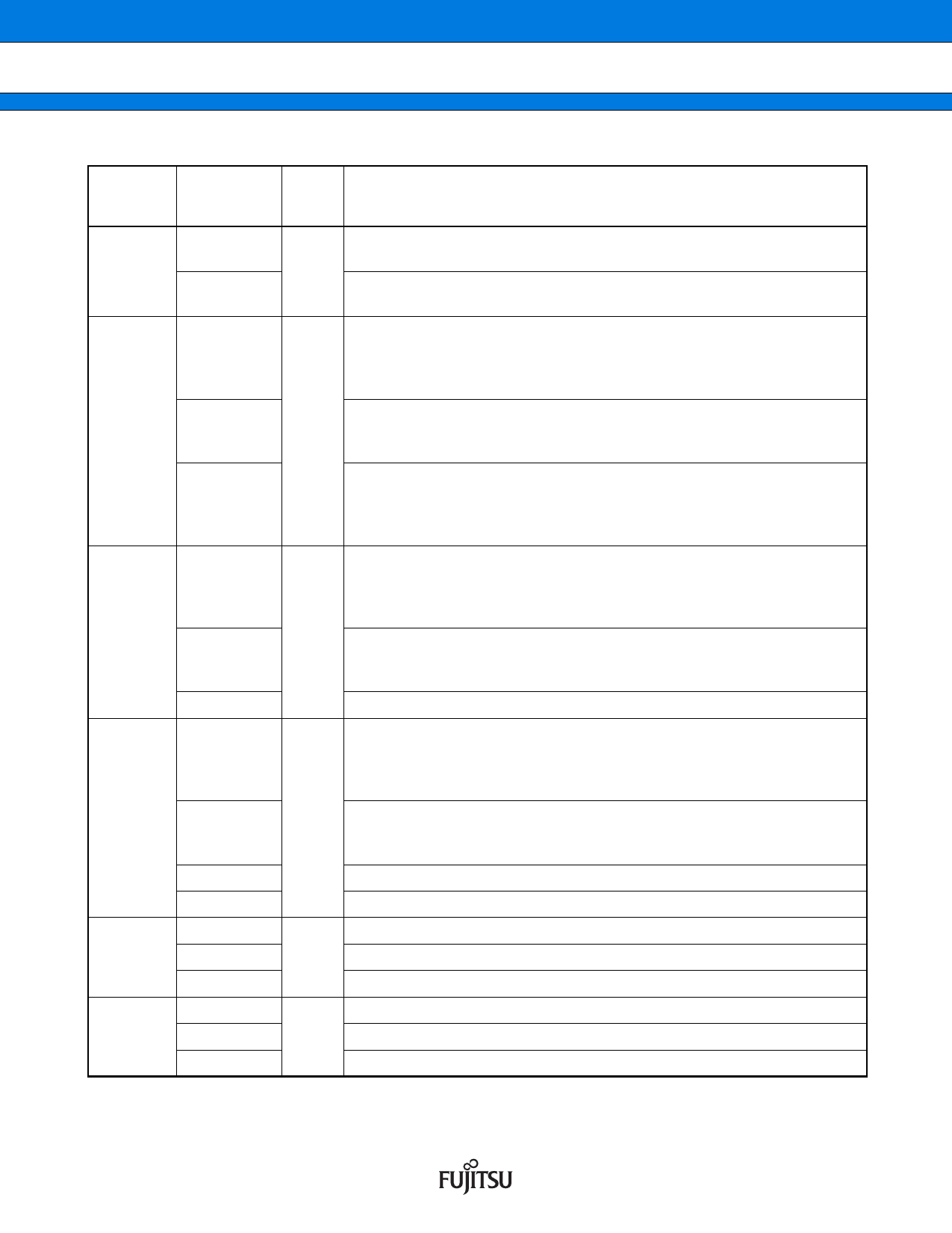
Pin No.
39
40 to 43
44
51
52
53
Pin name
P17
AD15
P20 to P23
A16 to A19
PPG9 (8)
PPGB (A)
PPGD (C)
PPGF (E)
P24
A20
IN0
P25
A21
IN1
ADTG
P44
SDA0
FRCK0
P45
SCL0
FRCK1
I/O
Circuit
type*
Function
General purpose I/O port. The register can be set to select whether to use
a pull-up resistor. This function is enabled in single-chip mode.
G
Input/output pin for external bus address data bus bit 15.
This function is enabled when external bus is enabled.
General purpose I/O ports. The register can be set to select whether to use
a pull-up resistor. In external bus mode, the pins are enabled as a general-
purpose I/O port when the corresponding bit in the external address output
control register (HACR) is 1.
Output pins for A16 to A19 of the external address data bus.
G When the corresponding bit in the external address output control register
(HACR) is 0, the pins are enabled as high address output pins A16 to A19.
Output pins for PPGs
General purpose I/O port. The register can be set to select whether to use
a pull-up resistor. In external bus mode, the pin is enabled as a general-
purpose I/O port when the corresponding bit in the external address output
control register (HACR) is 1.
G Output pin for A20 of the external address data bus. When the correspond-
ing bit in the external address output control register (HACR) is 0, the pin is
enabled as high address output pin A20.
Data sample input pin for input capture ICU0
General purpose I/O port. The register can be set to select whether to use
a pull-up resistor. In external bus mode, the pin is enabled as a general-
purpose I/O port when the corresponding bit in the external address output
control register (HACR) is 1.
G Output pin for A21 of the external address data bus. When the correspond-
ing bit in the external address output control register (HACR) is 0, the pin is
enabled as high address output pin A21.
Data sample input pin for input capture ICU1
Trigger input pin for A/D converter
General purpose I/O port
H Serial data I/O pin for I2C 0
Input pin for the 16-bit Free-run Timer 0
General purpose I/O port
H Serial clock I/O pin for I2C 0
Input pin for the 16-bit Free-run Timer 1
(Continued)
DS07-13744-4E
17
Share Link: 