MB90350E Ver la hoja de datos (PDF) - Fujitsu
Número de pieza
componentes Descripción
Fabricante
MB90350E Datasheet PDF : 92 Pages
| |||
MB90350E Series
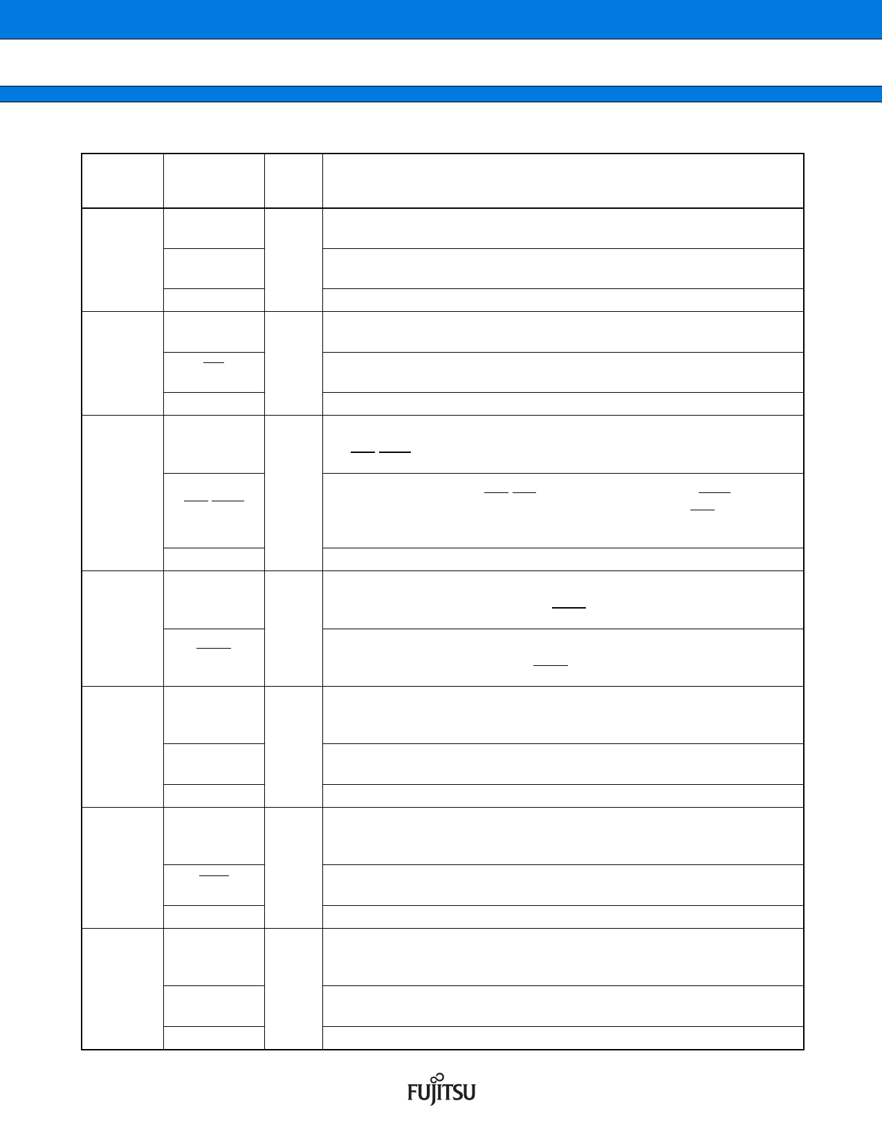
Pin No.
54
55
56
57
58
59
60
18
Pin name
P30
ALE
IN4
P31
RD
IN5
P32
WR/WRL
INT10R
P33
WRH
P34
HRQ
OUT4
P35
HAK
OUT5
P36
RDY
OUT6
I/O
Circuit
type*
Function
General purpose I/O port. The register can be set to select whether to use
a pull-up resistor. This function is enabled in single-chip mode.
G Address latch enable output pin. This function is enabled when external bus
is enabled.
Data sample input pin for input capture ICU4
General purpose I/O port. The register can be set to select whether to use
a pull-up resistor. This function is enabled in single-chip mode.
G Read strobe output pin for data bus. This function is enabled when external
bus is enabled.
Data sample input pin for input capture ICU5
General purpose I/O port. The register can be set to select whether to use
a pull-up resistor. This function is enabled either in single-chip mode or with
the WR/WRL pin output disabled.
G
Write strobe output pin for the data bus. This function is enabled when both
the external bus and the WR/WRL pin output are enabled. WRL is used to
write-strobe 8 lower bits of the data bus in 16-bit access. WR is used to
write-strobe 8 bits of the data bus in 8-bit access.
External interrupt request input pin for INT10
General purpose I/O port. The register can be set to select whether to use
a pull-up resistor. This function is enabled either in single-chip mode, in
external bus 8-bit mode or with the WRH pin output disabled.
G
Write strobe output pin for the 8 higher bits of the data bus. This function is
enabled when the external bus is enabled, when the external bus 16-bit
mode is selected, and when the WRH output pin is enabled.
General purpose I/O port. The register can be set to select whether to use
a pull-up resistor. This function is enabled either in single-chip mode or with
the hold function disabled.
G Hold request input pin. This function is enabled when both the external bus
and the hold function are enabled.
Wave form output pin for output compare OCU4
General purpose I/O port. The register can be set to select whether to use
a pull-up resistor. This function is enabled either in single-chip mode or with
the hold function disabled.
G Hold acknowledge output pin. This function is enabled when both the
external bus and the hold function are enabled.
Wave form output pin for output compare OCU5
General purpose I/O port. The register can be set to select whether to use
a pull-up resistor. This function is enabled either in single-chip mode or with
the external ready function disabled.
G Ready input pin. This function is enabled when both the external bus and
the external ready function are enabled.
Wave form output pin for output compare OCU6
(Continued)
DS07-13744-4E
Share Link: 