MAX4731 Ver la hoja de datos (PDF) - Maxim Integrated
Número de pieza
componentes Descripción
Fabricante
MAX4731 Datasheet PDF : 14 Pages
| |||
50Ω, Dual SPST Analog Switches in UCSP
ABSOLUTE MAXIMUM RATINGS
(All voltages referenced to GND.)
V+ ...........................................................................-0.3V to +12V
IN_, COM_, NO_, NC_ (Note 1)....................-0.3V to (V+ + 0.3V)
Continuous Current (any pin) ...........................................±10mA
Peak Current (any pin, pulsed at 1ms, 10% duty cycle) ...±20mA
Continuous Power Dissipation (TA = +70°C)
8-Pin µMAX (derate 4.5mW/°C above +70°C) .............362mW
8-Pin TDFN (derate 24.4mW/°C above +70°C) .........1951mW
9-Bump UCSP (derate 4.7mW/°C above +70°C).........379mW
Operating Temperature Range ...........................-40°C to +85°C
Storage Temperature Range .............................-65°C to +150°C
Maximum Junction Temperature .....................................+150°C
Lead Temperature (soldering, 10s) .................................+300°C
Bump Temperature (soldering, Note 2)
Infrared (15s) ...............................................................+220°C
Vapor Phase (60s) .......................................................+215°C
Note 1: Signals on IN_, NO_, NC_, or COM_ exceeding V+ or GND are clamped by internal diodes. Limit forward-diode current to
maximum current rating.
Note 2: This device is constructed using a unique set of packaging techniques that impose a limit on the thermal profile the device
can be exposed to during board level solder attach and rework. This limit permits only the use of the solder profiles recom-
mended in the industry-standard specification, JEDEC 020A, paragraph 7.6, Table 3 for IR/VPR and Convection reflow. Pre-
heating is required. Hand or wave soldering is not allowed.
Stresses beyond those listed under “Absolute Maximum Ratings” may cause permanent damage to the device. These are stress ratings only, and functional
operation of the device at these or any other conditions beyond those indicated in the operational sections of the specifications is not implied. Exposure to
absolute maximum rating conditions for extended periods may affect device reliability.
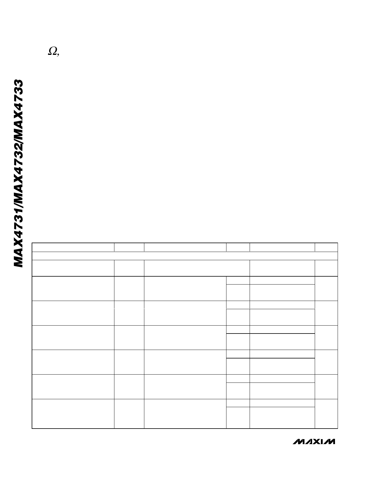
ELECTRICAL CHARACTERISTICS—Single +3V Supply
(V+ = +3V ±10%, VIH = +2.0V, VIL = +0.8V, TA = TMIN to TMAX, unless otherwise noted. Typical values are at V+ = +3V, TA = +25°C.)
(Notes 3, 4)
PARAMETER
ANALOG SWITCH
SYMBOL
CONDITIONS
TA
MIN
Analog Signal Range
VCOM_,
VNO_, VNC_
0
On-Resistance
RON
V+ = +2.7V,
ICOM_ = 5mA;
VNO_ or VNC_ = +1.5V
+25°C
TMIN to
TMAX
On-Resistance Matching
Between Channels (Notes 5, 6)
On-Resistance Flatness
(Note 7)
∆RON
V+ = +2.7V,
ICOM_ = 5mA;
VNO_ or VNC_ = +1.5V
V+ = +2.7V,
RFLAT(ON) ICOM_ = 5mA;
VNO_ or VNC_ = +1V, +1.5V, +2V
+25°C
TMIN to
TMAX
+25°C
TMIN to
TMAX
NO_ or NC_ Off-Leakage Current
(Note 8)
INO_(OFF)
INC_(OFF)
V+ = +3.6V,
VCOM_ = +0.3V, +3V;
VNO_ or VNC_ = +3V, +0.3V
COM_ Off-Leakage Current
(Note 8)
V+ = +3.6V,
ICOM_(OFF) VCOM_ = +0.3V, +3V;
VNO_ or VNC_ = +3V, +0.3V
+25°C -0.1
TMIN to
-2
TMAX
+25°C -0.1
TMIN to
-2
TMAX
COM_ On-Leakage Current
(Note 8)
ICOM_(ON)
V+ = +3.6V,
VCOM_ = +0.3V, +3.0V;
VNO_ or VNC_ = +0.3V, +3V, or
floating
+25°C -0.2
TMIN to
TMAX
-4
TYP MAX UNITS
V+
V
19
50
Ω
60
0.8
3.5
Ω
4.5
2.3
9
Ω
11
+0.1
nA
+2
+0.1
nA
+2
+0.2
nA
+4
2 _______________________________________________________________________________________
Share Link: 