M35500 Ver la hoja de datos (PDF) - MITSUBISHI ELECTRIC
Número de pieza
componentes Descripción
Fabricante
M35500 Datasheet PDF : 16 Pages
| |||
MITSUBISHI <DIGITAL ASSP>
M35500AFP/BGP
FLD(VFD) CONTROLLER
PIN DESCRIPTION
Table. 1. Pin description
Pin
Name
Input
Output
VCC, VSS
VEE
XIN
XOUT
______
RESET
Power source
Pull-down
power source
Clock input Input
Clock output
Output
______
RESET input CMOS input
____
CS
Chip select CMOS input
SCLK
Serial clock CMOS input
Noise filter
SOUT
Serial output
N-channel
open-drain
SIN
Serial input CMOS input
Noise filter
DIG0/P0 –
DIG7/P7
Digit/Port
P-channel
open-drain
DIG8/SEG17 – Digit/Segment
DIG17/SEG8
P-channel
open-drain
SEG0 – SEG7 Segment
P-channel
open-drain
Function
• Apply voltage of 5 V to VCC, and 0 V to VSS.
• Applies voltage supplied to pull-down resistors.
• RC oscillator pins for system clock.
• Reset input pin for active “L”.
• Internal pull-up resistors connected between the RESET and VCC pins.
• Serial transfer is possible by inputting “L” signal.
• Clock for serial transfer is input.
• Read a clock twice with 2 MHz sampling clock and judge if it is a noise or not.
• Serial data is output.
• During reset it is in high-impedance state.
• Serial data is input.
• Read a clock twice with 2 MHz sampling clock and judge if it is a noise or not.
• Pin for ordinary output or digit output.
• At reset this port is set to VEE level through a pull-down resistor.
• Pin for digit output or segment output.
• At reset this port is set to VEE level through a pull-down resistor.
• Pin for segment output.
• At reset this port is set to VEE level through a pull-down resistor.
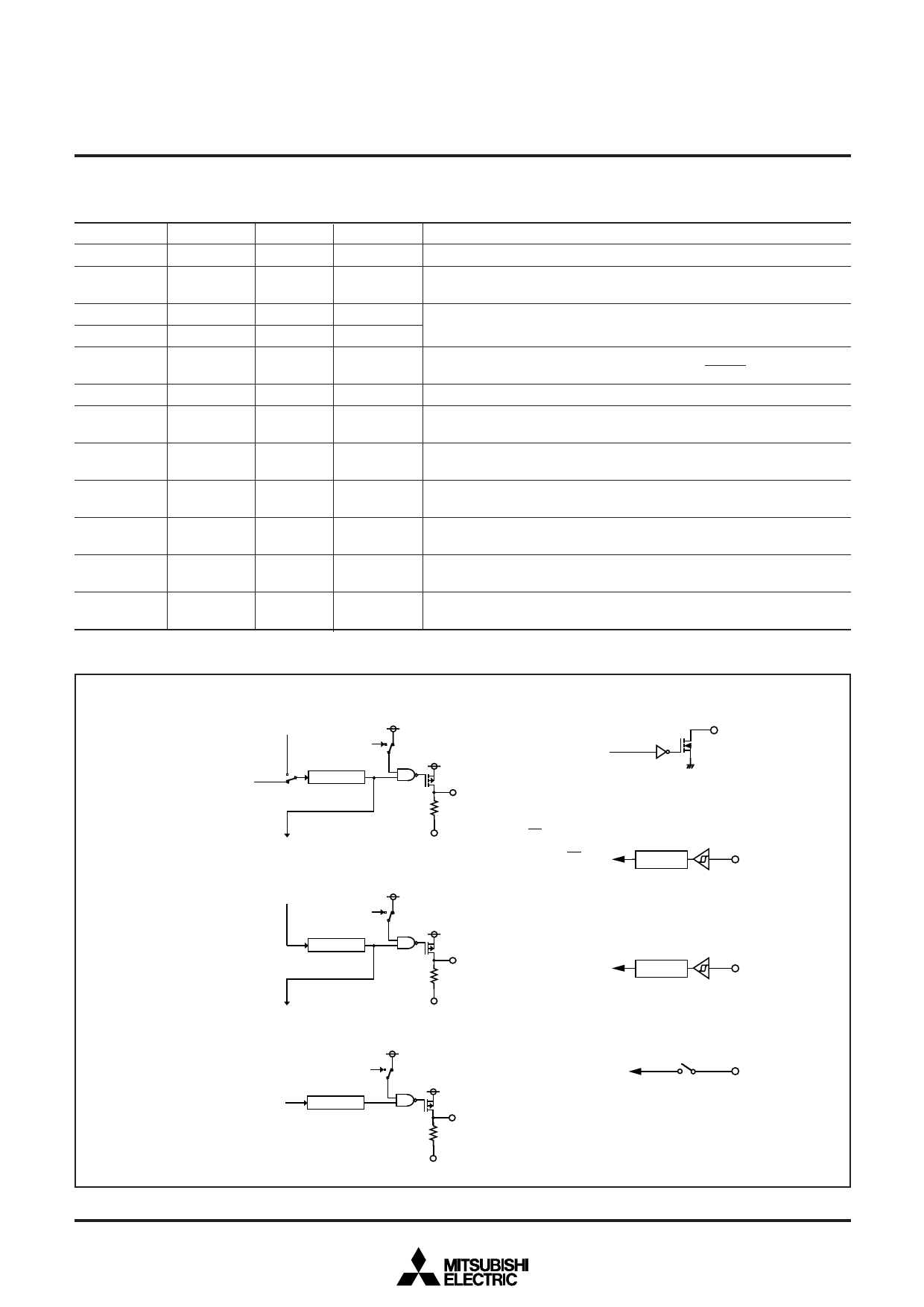
PORT BLOCK
(1) Digit/Port pin
Digit/Segment pin
Shift signal from high-order
Dimmer signal
(Note)
Data bus
latch
Segment data
(4) SOUT pin
SOUT signal
V
Shift signal to low-order
VEE
(2) Digit pin
Shift signal from high-order
Dimmer signal
(Note)
latch
V
Shift signal to low-order
VEE
(3) Segment pin
Dimmer signal
(Note)
Segment data
latch
V
(5) CS pin
CS input
Noise filter
(6) SIN, SCLK pin
Serial input
Serial clock input
Noise filter
(7) A-D input
A-D conversion input
Fig. 3. Port block diagram
V High-breakdown-voltage P-channel transistor
VEE
Note: Dimmer signal is for setting the Toff time.
3
Share Link: 