LT5528 Ver la hoja de datos (PDF) - Linear Technology
Número de pieza
componentes Descripción
Fabricante
LT5528 Datasheet PDF : 16 Pages
| |||
LT5528
APPLICATIO S I FOR ATIO
The RF output S22 with no LO power applied is given in
Table 4.
Table 4. RF Port Output Impedance vs Frequency for EN = High
and No LO Power Applied
Frequency
MHz
1000
1400
1600
1800
2000
2200
2400
2600
Output Impedance
Ω
23.7 + j8.1
37.7 + j18.5
47.0 + j14.3
46.0 + j5.5
39.2 + j3.7
34.2 + j6.2
31.0 + j9.4
29.6 + j11.6
S22
Mag
Angle
0.371
157
0.248
112
0.149
93.6
0.071
123
0.127
159
0.201
154
0.260
147
0.292
142
For EN = Low the S22 is given in Table 5.
Table 5. RF Port Output Impedance vs Frequency for EN = Low
Frequency Output Impedance
MHz
Ω
S22
Mag
Angle
1000
22.8 + j7.7
0.386
158
1400
32.4 + j20.8
0.321
116
1600
42.4 + j25.1
0.274
91.7
1800
54.6 + j20.1
0.193
66.2
2000
55.3 + j6.0
0.076
45.3
2200
44.7 + j0.0
0.056
180
2400
36.0 + j1.9
0.164
171
2600
31.3 + j4.8
0.237
162
To improve S22 for lower frequencies, a shunt capacitor
can be added to the output. At higher frequencies, a shunt
inductor can improve the S22. Figure 5 shows the equivalent
circuit schematic of the RF output.
Note that an ESD diode is connected internally from
the RF output to ground. For strong output RF signal
levels (higher than 3dBm), this ESD diode can degrade
the linearity performance if the 50Ω termination imped-
ance is connected directly to ground. To prevent this, a
VCC
RF
OUTPUT
20pF
3nH
21pF 52.5Ω
5528 F05
Figure 5. Equivalent Circuit Schematic of the RF Output
coupling capacitor can be inserted in the RF output line.
This is strongly recommended during a 1dB compression
measurement.
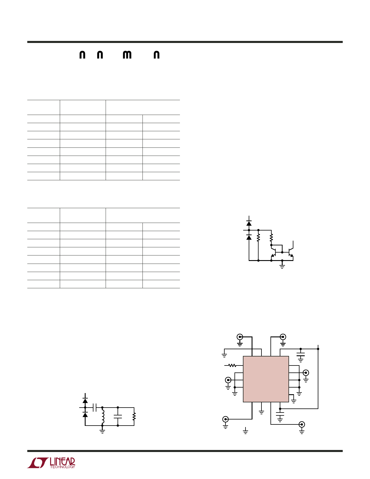
Enable Interface
Figure 6 shows a simplified schematic of the EN pin in-
terface. The voltage necessary to turn on the LT5528 is
1V. To disable (shut down) the chip, the Enable voltage
must be below 0.5V. If the EN pin is not connected, the
chip is disabled. This EN = Low condition is guaranteed
by the 75k on-chip pull-down resistor. It is important that
the voltage at the EN pin does not exceed VCC by more
than 0.5V. If this should occur, the supply current could
be sourced through the EN pin ESD protection diodes,
which are not designed to carry the full supply current,
and damage may result.
VCC
EN
75k 25k
5528 F06
Figure 6. EN Pin Interface
Evaluation Board
Figure 7 shows the evaluation board schematic. A good
ground connection is required for the exposed pad. If this
is not done properly, the RF performance will degrade.
J1
BBIM
J2
BBIP
VCC
16 15 14 13
VCC EN
R1
100Ω 1
BBMI GND BBPI VCC
12
EN
GND
J4
LO
IN
2
GND
3
LO
4
GND
LT5528
11
RF
10
GND
9
GND
17
GND
BBMQ GND BBPQ VCC
5678
C2
100nF
J3
RF
OUT
J5
BBQM
GND
C1
100nF
J6
BBQP
BOARD NUMBER: DC729A
5528 F07
Figure 7. Evaluation Circuit Schematic
5528f
11
Share Link: 