LH28F640SP Ver la hoja de datos (PDF) - Sharp Electronics
NГәmero de pieza
componentes DescripciГіn
Fabricante
LH28F640SP Datasheet PDF : 45 Pages
| |||
LHF64P01
15
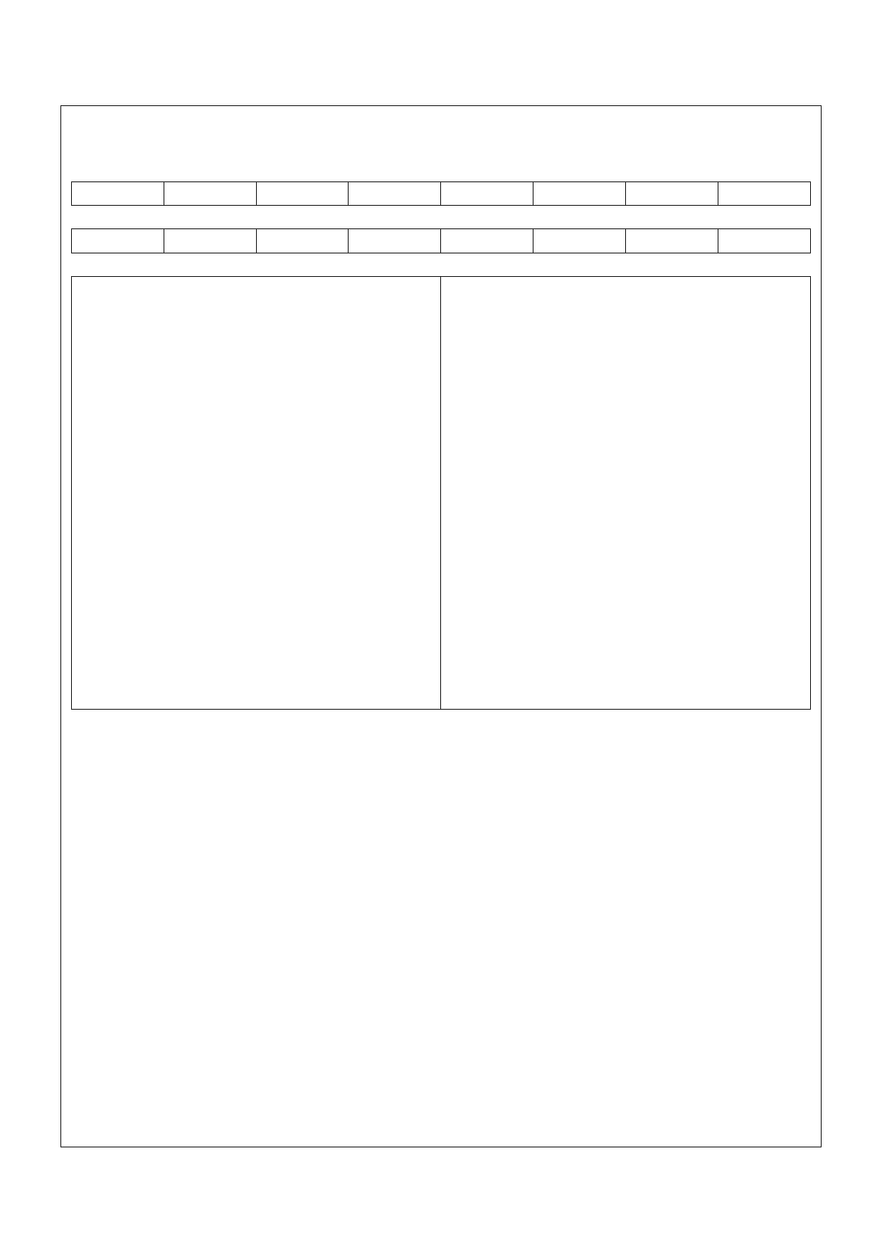
Table 9. STS Configuration Definition (1)
R
R
R
R
15
14
13
12
R
R
R
R
7
6
5
4
DQ15-DQ2 = RESERVED FOR FUTURE
ENHANCEMENTS (R)
DQ1-DQ0 = STS CONFIGURATION CODE (CC)
00 = level mode: RY/BY# indication. (Default)
01 = pulse mode on erase complete.
10 = pulse mode on program complete.
11 = pulse mode on erase or program complete.
R
R
R
R
11
10
9
8
R
R
CC
CC
3
2
1
0
NOTES:
After power-up or device reset, STS configuration is set to
"00".
STS configuration 00
The output of the STS pin is the control signal to prevent
accessing a flash memory while the internal WSM is busy
(SR.7="0").
In STS configuration = "00", STS is VOL when the WSM is STS configuration 01
executing internal erase or program algorithms.
The output of the STS pin is the control signal to indicate
that the erase operation is completed and the flash memory
STS configuration codes "01", "10" and "11" are all pulse is available for the next operation.
modes such that the STS pin pulses low then high when the
operation indicated by the configuration code is completed. STS configuration 10
The output of the STS pin is the control signal to indicate
that the program operation is completed and the flash
memory is available for the next operation.
STS configuration 11
The output of the STS pin is the control signal to indicate
that the erase or program operation is completed and the
flash memory is available for the next operation.
NOTE:
1. When the device is configured in one of the pulse modes, the STS pin pulses low with a typical pulse width of 250ns.
Rev. 0.06
Share Link: 