HIP6521(2000) Ver la hoja de datos (PDF) - Intersil
Número de pieza
componentes Descripción
Fabricante
HIP6521 Datasheet PDF : 13 Pages
| |||
HIP6521
Modulator Break Frequency Equations
FLC=
-------------------1--------------------
2π × LO × CO
FESR= 2----π-----×-----E----S--1---R------×----C-----O---
The compensation network consists of the error amplifier
(internal to the HIP6521) and the impedance networks ZIN
and ZFB. The goal of the compensation network is to provide
a closed loop transfer function with high 0dB crossing
frequency (f0dB) and adequate phase margin. Phase margin
is the difference between the closed loop phase at f0dB and
180 degrees. The equations below relate the compensation
network’s poles, zeros and gain to the components (R1, R2,
R3, C1, C2, and C3) in Figure 6. Use these guidelines for
locating the poles and zeros of the compensation network:
1. Pick Gain (R2/R1) for desired converter bandwidth
2. Place 1ST Zero Below Filter’s Double Pole (~75% FLC)
3. Place 2ND Zero at Filter’s Double Pole
4. Place 1ST Pole at the ESR Zero
5. Place 2ND Pole at Half the Switching Frequency
6. Check Gain against Error Amplifier’s Open-Loop Gain
7. Estimate Phase Margin - Repeat if Necessary
Compensation Break Frequency Equations
FZ1 = 2----π-----×-----R---1--2-----×----C-----1--
FZ2 = 2----π-----×-----(--R-----S----1---1-+-----R-----3----)---×-----C-----3--
FP1
=
---------------------------1---------------------------
2
π
×
R2
×
C-C----11-----+×-----CC-----22--
FP2 = 2----π-----×-----R---1--3-----×----C-----3--
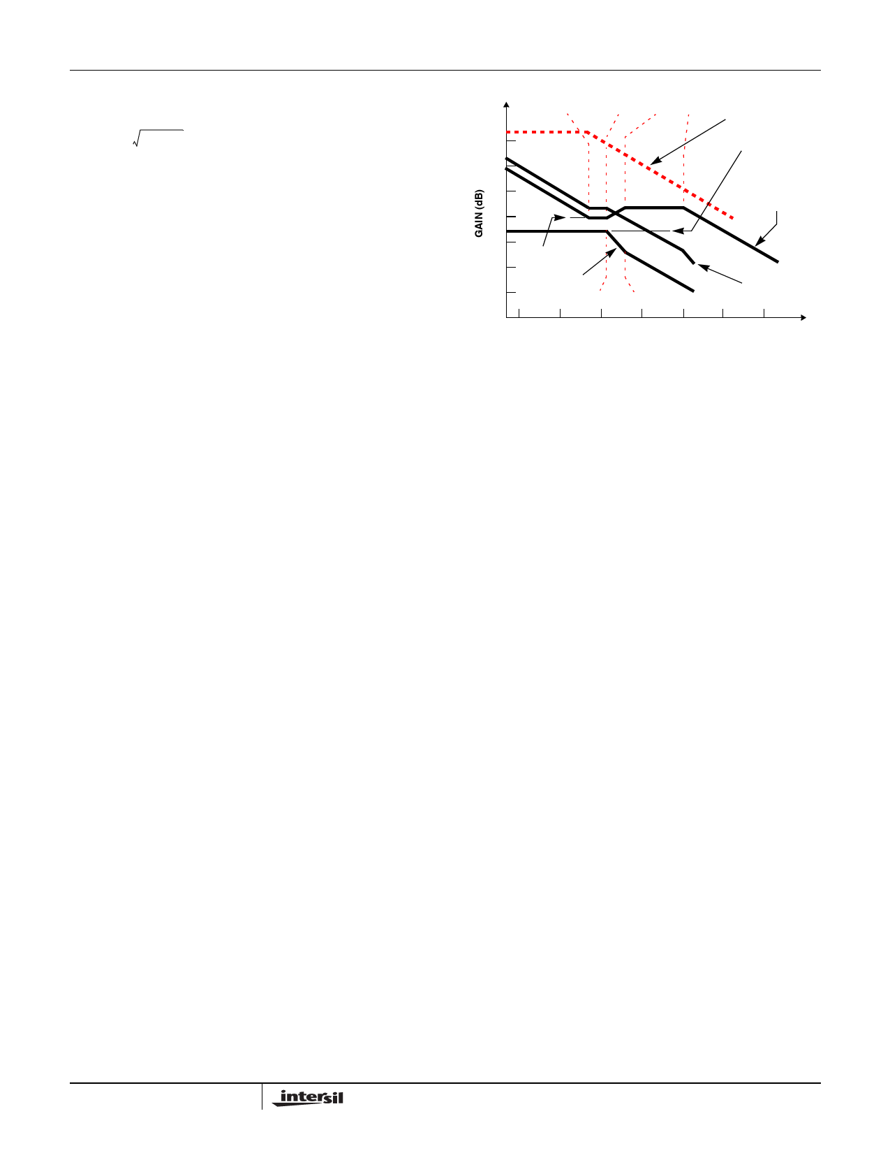
Figure 7 shows an asymptotic plot of the DC-DC converter’s
gain vs. frequency. The actual Modulator Gain has a high
gain peak dependent on the quality factor (Q) of the output
filter, which is not shown in Figure 6. Using the above
guidelines should yield a Compensation Gain similar to the
curve plotted. The open loop error amplifier gain bounds the
compensation gain. Check the compensation gain at FP2
with the capabilities of the error amplifier. The Closed Loop
Gain is constructed on the log-log graph of Figure 10 by
adding the Modulator Gain (in dB) to the Compensation Gain
(in dB). This is equivalent to multiplying the modulator
transfer function to the compensation transfer function and
plotting the gain.
The compensation gain uses external impedance networks
ZFB and ZIN to provide a stable, high bandwidth (BW) overall
loop. A stable control loop has a gain crossing with
-20dB/decade slope and a phase margin greater than 45
degrees. Include worst case component variations when
determining phase margin.
FZ1
FZ2 FP1 FP2
OPEN LOOP
100
ERROR AMP GAIN
80
20log V--V---P-I--N-P---
60
40
COMPENSATION
GAIN
20
0
-20
20
log
R--R----S--2--1--
MODULATOR
-40
GAIN
FLC FESR
CLOSED LOOP
GAIN
-60
10
100
1K
10K 100K 1M 10M
FREQUENCY (Hz)
FIGURE 7. ASYMPTOTIC BODE PLOT OF CONVERTER GAIN
ACPI Implementation
The three linear controllers included within the HIP6521 can
independently be shut down, in order to accommodate
Advanced Configuration and Power Interface (ACPI) power
management features.
To shut down any of the linears, one needs to pull and keep
high the respective FB pin above a typical threshold of
1.25V. One way to achieve this task is by using a logic gate
coupled through a small-signal diode. The diode should be
placed as close to the FB pin as possible to minimize stray
capacitance to this pin. Upon turn-off of the pull-up device,
the respective output undergoes a soft-start cycle, bringing
the output within regulation limits. On the regulators
implementing this feature, the parallel combination of the
feedback resistors has to be sufficiently high to allow ease of
driving from the external device. Considering the other
restriction applying to the upper range of this resistor
combination (see ‘Output Voltage Selection’ paragraph), it is
recommended the values of the feedback resistors on an
ACPI-enabled linear regulator output meet the following
constraint:
2kΩ < -RR----SS-----+×-----RR----P-P- < 5kΩ
To turn off the switching regulator, use an open-drain or
open-collector device capable of pulling the OCSET pin (with
the attached ROCSET pull-up) below 1.25V. To minimize the
possibility of OC trips at levels different than predicted, a
COCSET capacitor with a value of an order of magnitude
larger than the output capacitance of the pull-down device,
has to be used in parallel with ROCSET (1nF recommended).
Upon turn-off of the pull-down device, the switching regulator
undergoes a soft-start cycle.
Important
If the collector voltage to a linear regulator pass transistor
(Q3, Q4, or Q5) is lost, the respective regulator has to be
9
Share Link: 