HIP6521(2000) Ver la hoja de datos (PDF) - Intersil
Número de pieza
componentes Descripción
Fabricante
HIP6521 Datasheet PDF : 13 Pages
| |||
HIP6521
1. The maximum rDS(ON) at the highest junction temperature.
2. The minimum IOCSET from the specification table.
3. Determine IPEAK for IPEAK > IOUT(MAX) + (∆I)/2, where
∆I is the output inductor ripple current.
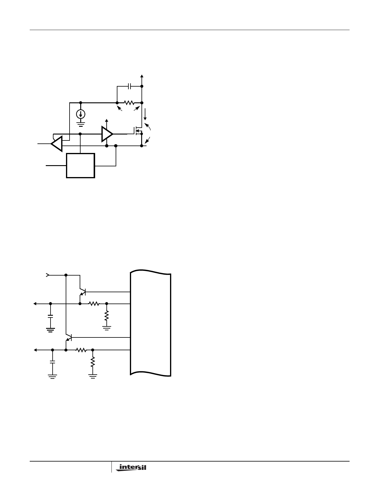
OVERCURRENT TRIP:
VDS > VSET
iD × rDS(ON) > IOCSET × ROCSET
OCSET
VIN = +5V
ROCSET
OC
+
-
OCC
PWM
IOCSET
40µA
DRIVE
GATE
CONTROL
VSET +
VCC
UGATE
PHASE
iD
+
VDS(ON)
VPHASE = VIN – VDS
VOCSET = VIN – VSET
FIGURE 3. OVERCURRENT DETECTION
For an equation for the ripple current see the section under
component guidelines titled ‘Output Inductor Selection’.
Output Voltage Selection
The output voltage of the PWM converter can be resistor-
programmed to any level between VIN and 0.8V. However,
since the value of RS1 is affecting the values of the rest of
the compensation components, it is advisable its value is
kept between 2kΩ and 5kΩ.
3.3VIN
VOUT3
+
COUT3
Q4
DRIVE3
FB3
RS3
RP3
HIP6521
Q5
VOUT4
+
COUT4
DRIVE4
FB4
RS4
RP4
VOUT
=
0.8 ×
1
+
RR-----SP--
FIGURE 4. ADJUSTING THE OUTPUT VOLTAGE OF ANY OF
THE FOUR REGULATORS (OUTPUTS 3 AND 4
PICTURED)
All linear regulators’ output voltages are set by means of
external resistor dividers as shown in Figure 4. The two
resistors used to set the voltage on each of the three linear
regulators have to meet the following criteria: their value
while in a parallel connection has to be less than 5kΩ, or
otherwise said, the following relationship has to be met:
-RR----SS-----+×-----RR----P-P- < 5kΩ
There may be a second restriction on the size of the
resistors used to set the linear regulators’ output voltage
based on ACPI functionality. Read the ‘ACPI
Implementation’ section under ‘Application Guidelines’ to
see if this additional constraint concerns your application. To
ensure the parallel combination of the feedback resistors
equals a certain chosen value, RFB, use the following
equations:
RS
=
V-----O----U----T--
VFB
×
RFB
RP = V----R-O----SU----T-×----–-V----VF----BF---B-- , where
VOUT - the desired output voltage,
VFB - feedback (reference) voltage, 0.8V.
Application Guidelines
Soft-Start Interval
The soft-start function controls the output voltages rate of rise
to limit the current surge at start-up. The soft-start function is
integrated on the chip and the soft-start interval is thus fixed.
Layout Considerations
MOSFETs switch very fast and efficiently. The speed with
which the current transitions from one device to another
causes voltage spikes across the interconnecting
impedances and parasitic circuit elements. The voltage
spikes can degrade efficiency, radiate noise into the circuit,
and lead to device overvoltage stress. Careful component
layout and printed circuit design minimizes the voltage
spikes in the converter. Consider, as an example, the turn-
off transition of the upper PWM MOSFET. Prior to turn-off,
the upper MOSFET was carrying the full load current.
During the turn-off, current stops flowing in the upper
MOSFET and is picked up by the lower MOSFET or
Schottky diode. Any inductance in the switched current
path generates a large voltage spike during the switching
interval. Careful component selection, tight layout of the
critical components, and short, wide circuit traces minimize
the magnitude of voltage spikes. See the Application Note
AN9908 for evaluation board drawings of the component
placement and printed circuit board.
There are two sets of critical components in a DC-DC
converter using a HIP6521 controller. The switching power
components are the most critical because they switch large
amounts of energy, and as such, they tend to generate
7
Share Link: 