FOD8012 Ver la hoja de datos (PDF) - Fairchild Semiconductor
Número de pieza
componentes Descripción
Fabricante
FOD8012 Datasheet PDF : 12 Pages
| |||
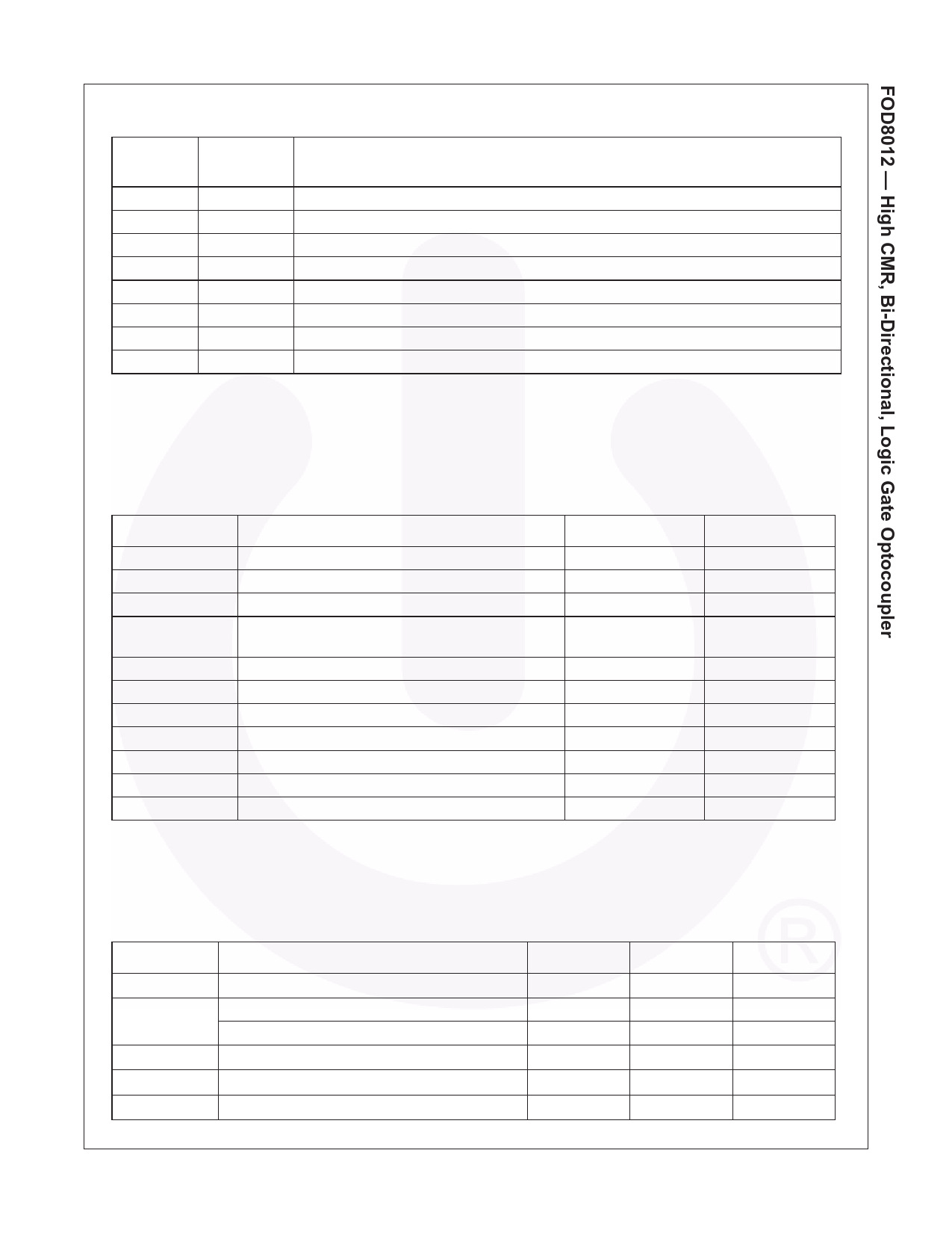
Pin Definitions
Pin
Number
1
2
3
4
5
6
7
8
Pin
Name
VDD1
VOA
VINB
GND1
GND2
VOB
VINA
VDD2
Description
Supply Voltage to Channel-A detector IC and Channel-B buffer IC
Output Voltage from Channel-A detector IC
Input Voltage to Channel-B buffer IC
Ground for Channel-A detector IC and Channel-B buffer IC
Ground for Channel-A buffer IC and Channel-B detector IC
Output Voltage from Channel-B detector IC
Input Voltage to Channel-A buffer IC
Supply Voltage to Channel-A buffer IC and Channel-B detector IC
Absolute Maximum Ratings (TA=25ºC unless otherwise specified)
Stresses exceeding the absolute maximum ratings may damage the device. The device may not function or be
operable above the recommended operating conditions and stressing the parts to these levels is not recommended.
In addition, extended exposure to stresses above the recommended operating conditions may affect device reliability.
The absolute maximum ratings are stress ratings only.
Symbol
TSTG
TOPR
TJ
TSOL
VDD1, VDD2
VIA, VIB
IIA, IIB
VOA, VOB
IOA, IOB
PDI
PDO
Parameter
Storage Temperature
Operating Temperature
Junction Temperature
Lead Solder Temperature
(Refer to Reflow Temperature Profile)
Supply Voltage
Input Voltage
Input DC Current
Output Voltage
Average Output Current
Input Power Dissipation(1)
Output Power Dissipation(1)
Value
-40 to +125
-40 to +110
-40 to +130
260 for 10sec
0 to 6.0
-0.5 to VDD+0.5
-10 to +10
-0.5 to VDD+0.5
10
60
60
Units
ºC
ºC
ºC
ºC
V
V
µA
V
mA
mW
mW
Recommended Operating Conditions
The Recommended Operating Conditions table defines the conditions for actual device operation. Recommended
operating conditions are specified to ensure optimal performance to the datasheet specifications. Fairchild does not
recommend exceeding them or designing to Absolute Maximum Ratings.
Symbol
Parameter
Min.
Max.
Unit
TA
VDD1, VDD2
VIH
VIL
tr, tf
Ambient Operating Temperature
Supply Voltages (3.3V Operation)(2)
Supply Voltages (5.0V Operation)(2)
Logic High Input Voltage
Logic Low Input Voltage
Input Signal Rise and Fall Time
-40
+110
ºC
3.0
3.6
V
4.5
5.5
V
2.0
VDD
V
0
0.8
V
1.0
ms
©2010 Fairchild Semiconductor Corporation
FOD8012 Rev. 1.0.5
2
www.fairchildsemi.com
Share Link: 