FDS6064N7 Ver la hoja de datos (PDF) - Fairchild Semiconductor
NГәmero de pieza
componentes DescripciГіn
Fabricante
FDS6064N7 Datasheet PDF : 6 Pages
| |||
Electrical Characteristics
Symbol
Parameter
TA = 25В°C unless otherwise noted
Test Conditions
Min Typ Max Units
Off Characteristics
BVDSS
DrainвҖ“Source Breakdown Voltage VGS = 0 V,
ID = 250 ВөA
20
вҲҶBVDSS
вҲҶTJ
Breakdown Voltage Temperature ID = 250 ВөA, Referenced to 25В°C
Coefficient
IDSS
Zero Gate Voltage Drain Current VDS = 16 V,
VGS = 0 V
IGSSF
GateвҖ“Body Leakage, Forward
VGS = 8 V,
VDS = 0 V
IGSSR
GateвҖ“Body Leakage, Reverse
VGS = вҖ“8 V , VDS = 0 V
V
11
mV/В°C
1
ВөA
100 nA
вҖ“100 nA
On Characteristics
(Note 2)
VGS(th)
Gate Threshold Voltage
вҲҶVGS(th)
вҲҶTJ
RDS(on)
Gate Threshold Voltage
Temperature Coefficient
Static DrainвҖ“Source
OnвҖ“Resistance
gFS
Forward Transconductance
VDS = VGS,
ID = 250 ВөA
0.4
0.6
1.5
V
ID = 250 ВөA, Referenced to 25В°C
вҖ“3
mV/В°C
VGS = 4.5 V, ID = 23 A
VGS = 2.5 V, ID = 22 A
VGS = 1.8 V, ID = 18 A
VGS = 4.5 V, ID = 23 A,TJ = 125В°C
VDS = 5 V,
ID = 23 A
2.2
3.5
mв„Ұ
2.7
4
3.4
6
3
5
179
S
Dynamic Characteristics
Ciss
Input Capacitance
Coss
Output Capacitance
Crss
Reverse Transfer Capacitance
RG
Gate Resistance
VDS = 10 V,
f = 1.0 MHz
V GS = 0 V,
VGS = 15 mV, f = 1.0 MHz
7191
pF
1403
pF
703
pF
1.2
в„Ұ
Switching Characteristics
td(on)
TurnвҖ“On Delay Time
tr
TurnвҖ“On Rise Time
td(off)
TurnвҖ“Off Delay Time
tf
TurnвҖ“Off Fall Time
Qg
Total Gate Charge
Qgs
GateвҖ“Source Charge
Qgd
GateвҖ“Drain Charge
(Note 2)
VDD = 10 V,
VGS = 4.5 V,
ID = 1 A,
RGEN = 6 в„Ұ
VDS = 10 V,
VGS = 4.5 V
ID = 23 A,
22
35
ns
22
35
ns
153 245
ns
77
123
ns
70
98
nC
10
nC
15
nC
DrainвҖ“Source Diode Characteristics and Maximum Ratings
IS
Maximum Continuous DrainвҖ“Source Diode Forward Current
VSD
DrainвҖ“Source Diode Forward
Voltage
VGS = 0 V, IS = 2.5 A
trr
Diode Reverse Recovery Time IF = 23 A,
Qrr
Diode Reverse Recovery Charge diF/dt = 100 A/Вөs
Notes:
(Note 2)
2.5
A
0.6
1.2
V
43
nS
55
nC
1. RОёJA is the sum of the junction-to-case and case-to-ambient thermal resistance where the case thermal reference is defined as the solder mounting surface of
the drain pins. RОёJC is guaranteed by design while RОёCA is determined by the user's board design.
a) 40В°C/W when
mounted on a 1in2 pad
of 2 oz copper
b) 85В°C/W when mounted on
a minimum pad of 2 oz
copper
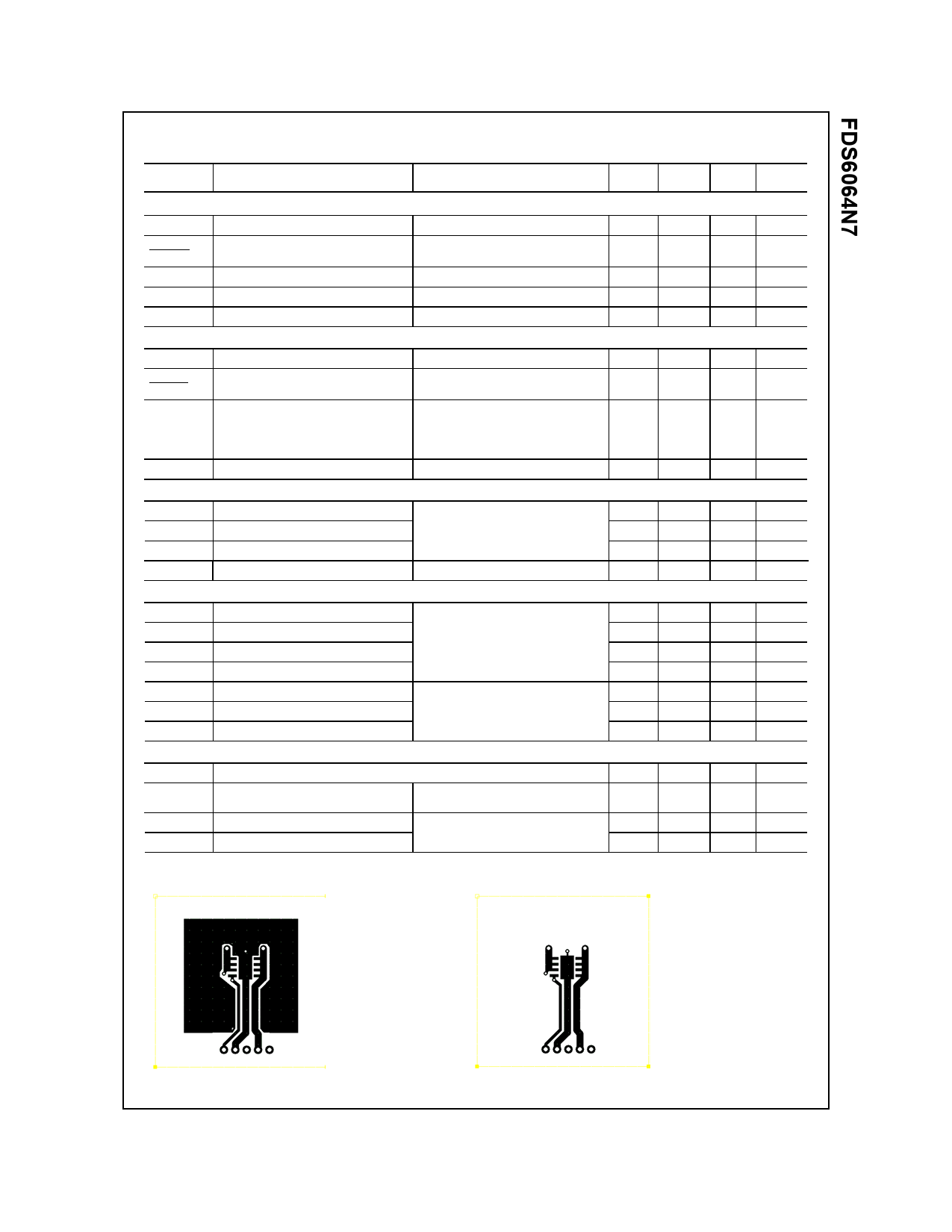
Scale 1 : 1 on letter size paper
2. Pulse Test: Pulse Width < 300Вөs, Duty Cycle < 2.0%
FDS6064N7 Rev D2 (W)
Share Link: 