EM83040BH Ver la hoja de datos (PDF) - ELAN Microelectronics
Número de pieza
componentes Descripción
Fabricante
EM83040BH Datasheet PDF : 22 Pages
| |||
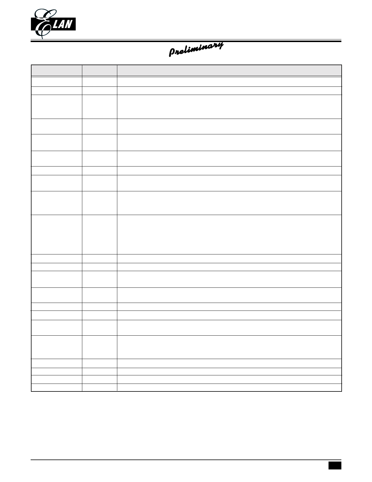
PIN DESCRIPTIONS
Symbol
I/O
VDD
GND
VOUT
Power
Power
Power
VSS4
VSS3
VSS2+
VSS2-
VREG
MAIN
Power
Power
Power
Power
Power
I
EN
I
M1
I
M0
I
RAMEN
RAMADS
RAMW
RAMR
RAMD3~RAM
D0
LOAD
I/O
CA
I
CB
I
V1~V5
I
O1~O80
O
Preliminary
EM83040B
LCD CONTROLLER
Function
System power supply
Ground
Voltage converter input/output pin
Connect this pin to GND through capacitor
EN=1,VOUT=VDD
Step-up capacitor
EN=1, VSS4=VDD
Step-up capacitor
EN=1, VSS3=VDD
Step-up capacitor
EN=1, VSS2=VDD
Step-up capacitor
Output voltage regulator terminal. Provides the voltage between V1 and GND
through a resistive voltage divider.
Master or slave control signal.
MAIN=1, master unit
MAIN=0, slave unit
This pin control whole chip power. This chip will work when this pin is connected
to ground. And whole chip will disable when connect to VDD voltage.
EN=0 and MAIN=1 the chip will generate VSS2+, VSS2-
VSS3, VSS4, VOUT, LOAD signal and internal RC clock.
EN=1, standby mode
Mode select
Mode select
RAM read and write control signal.
1 => can not read and write. 0=> can read and write.
RAM data select signal
1=> RAM Data, 0=>Address
RAM write signal, low write
RAM read signal, low read
RAM data or address bus
LCD load signal between one COMMON signal to another.
MAIN=1, the master unit will output LOAD signal.
MAIN=0, the slave will accept the signal from master unit.
Coupling capacitor
Coupling capacitor
Reference voltage input, highest V1°K lowest V5
LCD waveform output
* This specification are subject to be changed without notice.
9.14.2001 5
Share Link: 