EM83040BH Ver la hoja de datos (PDF) - ELAN Microelectronics
Número de pieza
componentes Descripción
Fabricante
EM83040BH Datasheet PDF : 22 Pages
| |||
EM83040B
LCD CONTROLLER
Preliminary
Address 2560 bit3 (IRS) is internal resistor selected
IRS=0: internal regulator resistor is used.
IRS=1: internal regulator resistor is not used. (External resistor is used)
Address 2560 bit0~2(IR2, IR1, IR0) is selected for the V1 voltage regulator internal resistance ratio
IR2~IR0
Resistor ratio (1+Rb/Ra)
000
3.0
001
3.5
010
4.0
011
4.5
100
5.0
101
5.5
110
6.0
111
6.5
The V1 voltage can be calculated using equation A over the range where VDD < V1 ≤ VOUT
V1=(1+Rb/Ra) • VEV *(94%~97%) (Equation A)
(94%~97%) depend on loading
Example: Default: IRS=0 (internal regulator resistor is used), (IR2, IR1, IR0)=(0, 1, 0), and (REG5~0)=(000000)
V1=(1+Rb/Ra) • VEV*(94%~97%)=4.0 • 1.2*(94%~97%)= 4.51 V~4.65V
When IRS=0 (internal regulator resistor is used), (IR2, IR1, IR0)=(0, 1, 1), and (REG5~0)=(100000)
V1=(1+Rb/Ra) • VEV*(94%~97%)=4.5 • 1.584*(94%~97%)= 6.7~6.91 V
FIG. 8 show the V1 voltage measured by values of the internal resistance ratio resistor (1+Rb/Ra) for V1 voltage
adjustment and electric volume resister (REG5~REG0).
FIG. 8 The output voltage V1 is determined by function of the V1 voltage regulator ratio register (1+Rb/Ra), and
the electric volume resister (REG5~REG0).
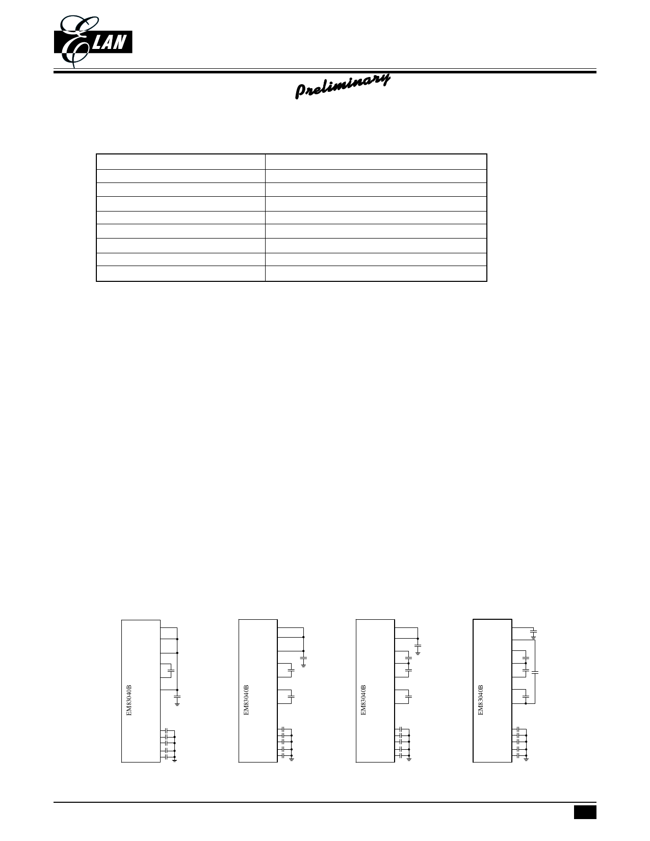
(8) The step-up voltage circuit
Case of the double step-up, the triple step-up and Case of the quad step-up VOUT is output voltage pin the bias
voltage V1 is supported from VREG.
(a) Double step-up, (b) Triple step-up, (c) Quad step-up (d) five times step-up C1=0.47 to 1.0£gf, C2=1.0 to
4.7uf
VOUT
VSS4
VSS3
CB
C2
CA
VSS2+
C2
VSS2-
VREG
C1
V1
V2
V3
V4
V5
VOUT
VSS4
VSS3
CB
CA
VSS2+
VSS2-
VREG
V1
V2
V3
V4
V5
C2
C2
C2
C1
VOUT
VSS4
VSS3
CB
CA
VSS2+
VSS2-
VREG
V1
V2
V3
V4
V5
C2
C2
C2
C2
C1
VOUT
C2
VSS4
VSS3
C2
CB
C2
CA
C2
VSS2+
C2
VSS2-
VREG
V1
V2
C1
V3
V4
V5
(a) VOUT=2*VDD (b) VOUT=3*VDD (c) VOUT=4*VDD
FIG. 9
* This specification are subject to be changed without notice.
(d) VOUT=5*VDD
9.14.2001 11
Share Link: 