DS2229 Ver la hoja de datos (PDF) - Dallas Semiconductor -> Maxim Integrated
Número de pieza
componentes Descripción
Fabricante
DS2229 Datasheet PDF : 10 Pages
| |||
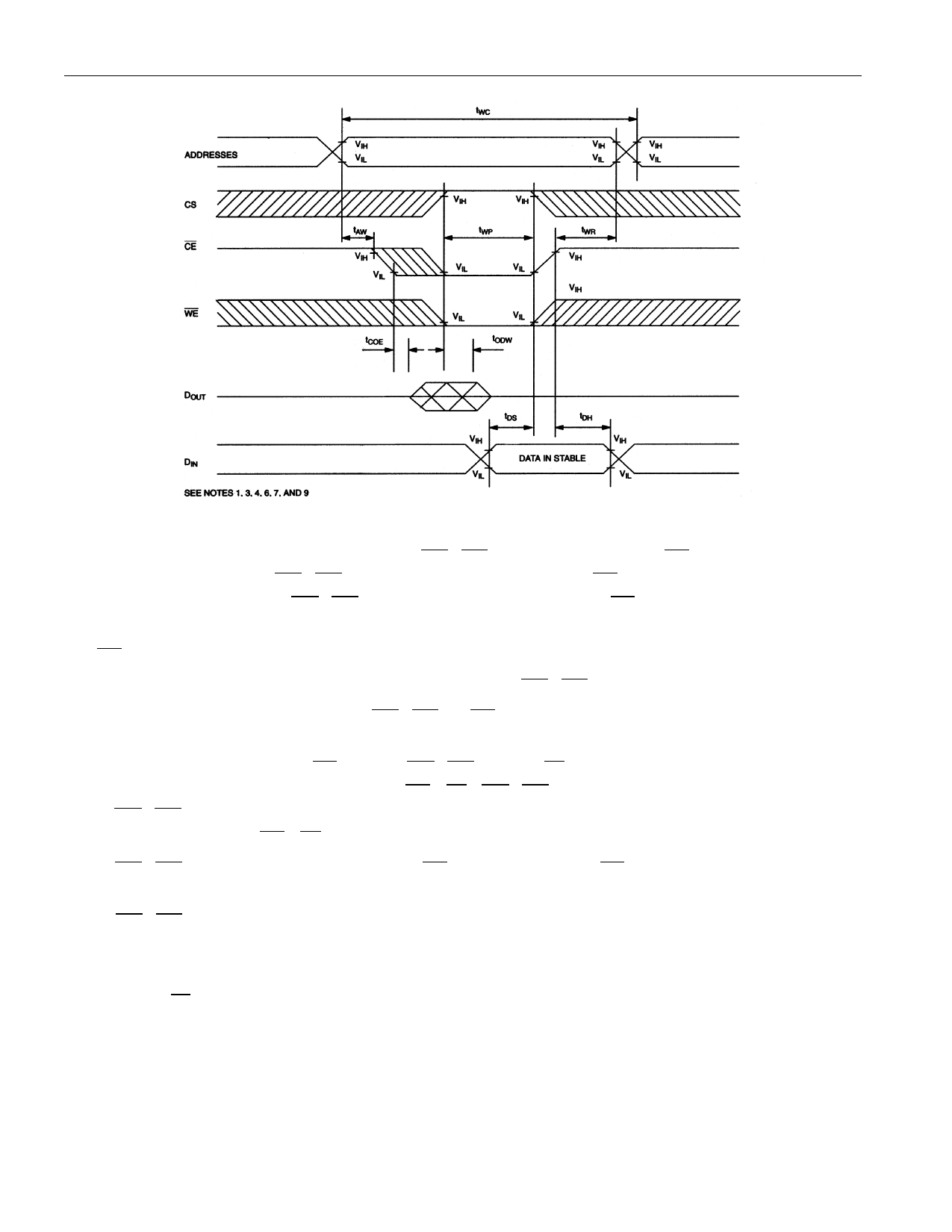
WRITE CYCLE 2 Figure 7
DS2229
NOTES:
1. A write occurs during the overlap of a low CE0 - CE3 , a high CS, and a low WE . A write begins at the
latest transition among CE0 - CE3 going low, CS going high, and WE going low. A write ends at the
earliest transition among CE0 - CE3 going high, CS going low and WE going high. tWP is measured
from the beginning of write to the end of write.
2. WE is high for a read cycle.
3. tDS ends and tDH begins at the earliest transaction among CE0 - CE3 going high.
4. tWR is measured from the earliest of CE0 - CE3 or WE going high or CS going low to the end of write
cycle.
5. CS controls address buffer, WE buffer, CE0 - CE3 buffer, OE buffer and DIN buffer. If CS controls
data retention mode, VIN levels (address, WE , OE , CE0 - CE3 , I/O) can be in the high impedance state.
If CE0 - CE3 controls data retention mode, CS must be CS ≥ VCC - 0.2V or 0V < CS < 0.2V. The other
input levels (address, WE , OE , I/O) can be in the high impedance state.
6. If CE0 - CE3 goes low simultaneously with WE going low or after WE going low, the outputs remain
in a high impedance state.
7. If CE0 - CE3 is low and CS is high during this period, I/O pins are in the output state. Therefore, the
input signals of the opposite phase to the outputs must not be applied to them.
8. This parameter is sampled and not 100% tested.
9. Only one CE active during any read or write cycle.
9 of 10
Share Link: 