SA7026DK Ver la hoja de datos (PDF) - Philips Electronics
Número de pieza
componentes Descripción
Fabricante
SA7026DK Datasheet PDF : 14 Pages
| |||
Philips Semiconductors
1.3GHz low voltage fractional-N dual synthesizer
Objective specification
SA7026
FUNCTIONAL DESCRIPTION
Main Fractional-N divider
The RFin input (pins 5 and 6) drive a pre-amplifier to provide the
clock to the first divider stage. For single ended operation, the signal
should be fed to one of the inputs while the other one is AC
grounded. The pre-amplifier has a high input impedance, dominated
by pin and pad capacitance. The circuit operates with signal levels
from –18dBm to +0dBm, and at frequencies as high as 2.5 GHz.
The divider consists of a fully programmable bipolar prescaler
followed by a CMOS counter. Divide ratios (512 to 65536) allow a
minimum phase comparison frequency of 25kHz at 2.5 GHz RF.
At the completion of a main divider cycle, a main divider output
pulse is generated which will drive the main phase comparator. Also,
the fractional accumulator is incremented by the value of NF. The
accumulator works with modulo Q set by FMOD. When the
accumulator overflows the overall division ratio N will be increased
by 1 to N + 1, the average division ratio over Q main divider cycles
(either 5 or 8) will be
NF
Nfrac + N ) Q
The output of the main divider will be modulated with a fractional
phase ripple. The phase ripple is proportional to the contents of the
fractional accumulator and is nulled by the fractional compensation
charge pump.
The reloading of a new programming word is synchronized to the
state of the main divider to avoid introducing a phase disturbance.
Auxiliary divider
The auxiliary divider consists of a divider with fully programmable
values between 128 and 16384. The AUXin input, pin 13, drives a
pre-amplifier to provide the clock to the first divider stage. The
AUXin negative input is internally connected to ground. The
pre-amplifier has a high input impedance, dominated by pin and pad
capacitance. The circuit operates with signal levels from –18dBm to
+0dBm (80 to 636 mVpp), and at frequencies as high as 550 MHz.
The divider consists of a fully programmable bipolar prescaler
followed by a CMOS counter. The divide ratios allow a minimum
phase comparison frequency of 25kHz at 550 MHz RF.
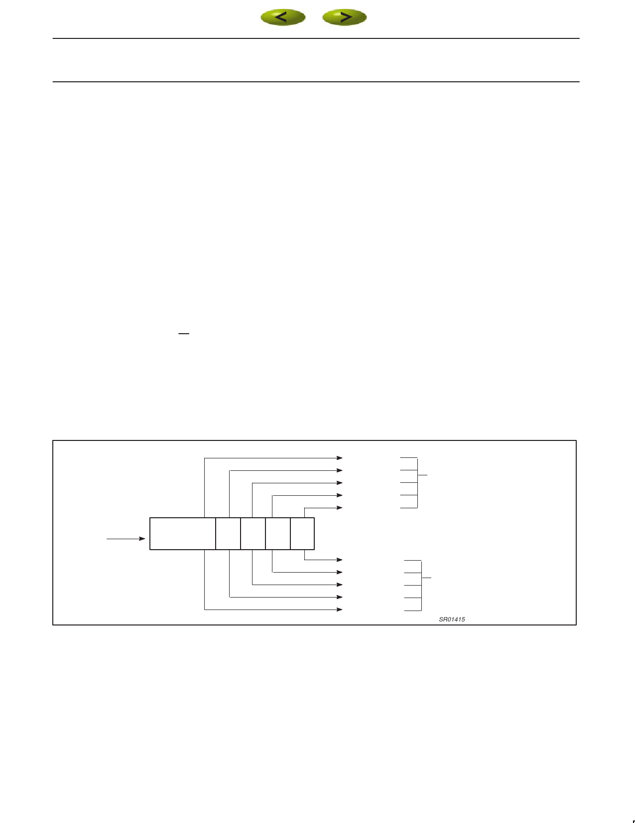
Reference divider
The reference divider consists of a divider with programmable
values between 4 and 1023 followed by a three bit binary counter.
The 3 bit SM (SA) register (see figure 4) determines which fo the 5
output pulses are selected as the main (auxiliary) phase detector
input.
Phase detector
The reference and main (aux) divider outputs are connected to a
phase/frequency detector that controls the charge pump. The pump
current is set by a an external resistor. The dead zone (caused by
finite time taken to switch the current sources on or off) is cancelled
by forcing the pumps ON for a minimum time at every cycle
(backlash time) providing improved linearity.
REFERENCE
INPUT
DIVIDE BY R
SM=”000”
SM=”001”
SM=”010”
SM=”011”
SM=”100”
/2
/2
/2
/2
SA=”100”
SA=”011”
SA=”010”
SA=”001”
SA=”000”
Figure 4. Reference Divider
MAIN
PHASE
DETECTOR
AUXILIARY
PHASE
DETECTOR
SR01415
1998 Oct 13
7
Share Link: 