CXA3086 Ver la hoja de datos (PDF) - Sony Semiconductor
Número de pieza
componentes Descripción
Fabricante
CXA3086 Datasheet PDF : 30 Pages
| |||
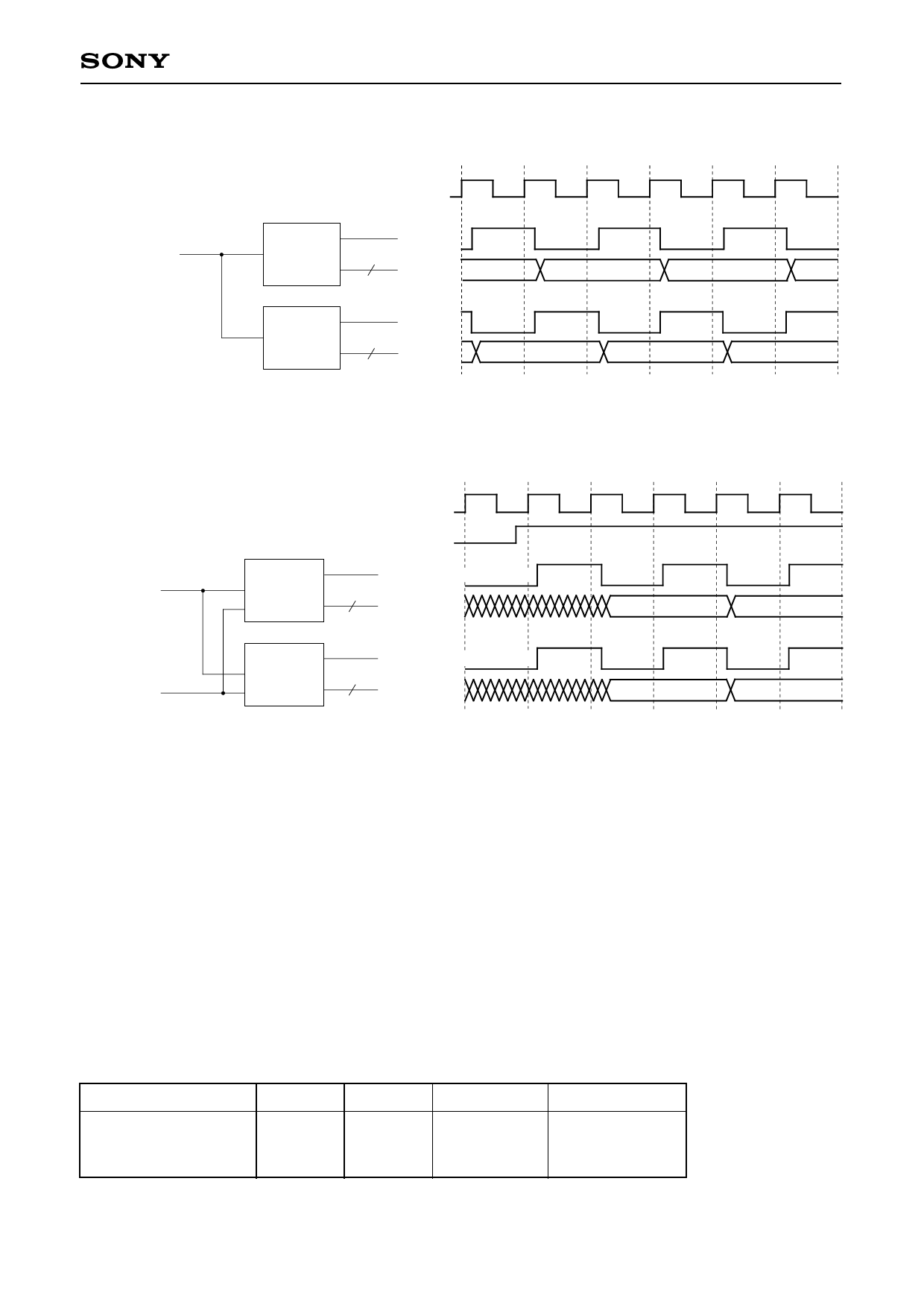
When the RESET signal is not used.
CLK
CLK
CXA3086Q
CLK A A
RESETN
CLKOUT
6bit
DATA
CXA3086Q
CLK B B
RESETN
CLKOUT
6bit
DATA
When the RESET signal is used.
CLK
RESET signal
CXA3086Q
CLK
A
RESETN
CLK
RESET signal
CLKOUT
6bit
DATA
(Reset period)
CXA3086Q
CLK
B
RESETN
CLKOUT
6bit
DATA
(Reset period)
CXA3086Q
2. Straight mode (See Application Circuits (4), (5) and (6).)
Set the SELECT pin to GND for this mode. In this mode, data output can be obtained in accordance with the
clock frequency applied to the A/D converter for applications which use the clock applied to the A/D converter
as the system clock.
The A/D converter can operate at Fc (min.) = 100MSPS in this mode.
Digital input level and supply voltage settings
The logic input level for the CXA3086Q supports ECL, PECL and TTL levels.
The power supplies (DVEE3, DGND3) for the logic input block must be set to match the logic input (CLK and
RESET signals) level.
Digital input level
ECL
PECL
TTL
DVEE3
–5V
0V
0V
DGND3
0V
+5V
+5V
Supply voltage Application circuits
±5V
(1) (4)
+5V
(2) (5)
+5V
(3) (6)
Table 3. Logic Input Level and Power Supply Settings
– 11 –
Share Link: 