CM3205 Ver la hoja de datos (PDF) - California Micro Devices Corp
Número de pieza
componentes Descripción
Fabricante
CM3205 Datasheet PDF : 10 Pages
| |||
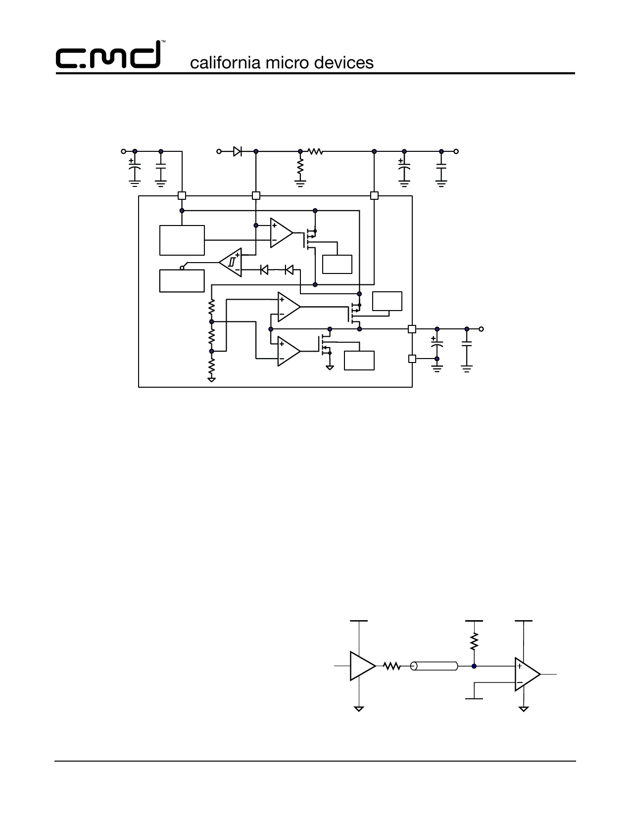
Functional Block Diagram
3.3V
S hut
Down
X) X)
9,1
$'-6'
5
5
9''4
PRELIMINARY
CM3205
2.50V, 5A
X)
X)
89/2
%DQGJDS
1.22V
273
6KXWGRZQ
9''4
CM3205
9''4
&XUUHQW
/LPLW
&XUUHQW
/LPLW
VDDQ/2, 2.5A
977
&XUUHQW
/LPLW
*1' X) X)
Application Information
Powering DDR Memory
Double-Data-Rate (DDR) memory has provided a huge
step in performance for personal computers, servers
and graphic systems. As is apparent in its name, DDR
operates at double the data rate of earlier RAM, with
two memory accesses per cycle versus one. DDR
SDRAM's transmit data at both the rising falling edges
of the memory bus clock.
DDR’s use of Stub Series Terminated Logic (SSTL)
topology improves noise immunity and power-supply
rejection, while reducing power dissipation. To achieve
this performance improvement, DDR requires more
complex power management architecture than previ-
ous RAM technology.
Unlike the conventional DRAM technology, DDR
SDRAM uses differential inputs and a reference volt-
age for all interface signals. This increases the data
bus bandwidth, and lowers the system power con-
sumption. Power consumption is reduced by lower
operating voltage, a lower signal voltage swing associ-
ated with Stub Series Terminated Logic (SSTL_2) and
by the use of a termination voltage, VTT. SSTL_2 is an
industry standard, defined in JEDEC document
JESD8-9. SSTL_2 maintains high-speed data bus sig-
nal integrity by reducing transmission reflections.
JEDEC further defines the DDR SDRAM specification
in JESD79C.
DDR memory requires three tightly regulated voltages:
VDDQ, VTT, and VREF (see Figure 1). In a typical
SSTL_2 receiver, the higher current VDDQ supply volt-
age is normally 2.5V with a tolerance of ±200-mV. The
active bus termination voltage, VTT, is half of VDDQ.
VREF is a reference voltage that tracks half of VDDQ, ±
1%, and is compared with the VTT terminated signal at
the receiver. VTT must be within ±40-mV of VREF.
VDDQ
VTT (=VDDQ/2) VDDQ
Rs = 25
Line
Rt = 25
Transmitter
VREF (=VDDQ/2)
Receiver
Figure 1. Typical DDR terminations, Class II
© 2006 California Micro Devices Corp. All rights reserved.
6 490 N. McCarthy Blvd., Milpitas, CA 95035-5112 l Tel: 408.263.3214 l Fax: 408.263.7846 l www.cmd.com
05/08/06
Share Link: 