CM3205 Ver la hoja de datos (PDF) - California Micro Devices Corp
Número de pieza
componentes Descripción
Fabricante
CM3205 Datasheet PDF : 10 Pages
| |||
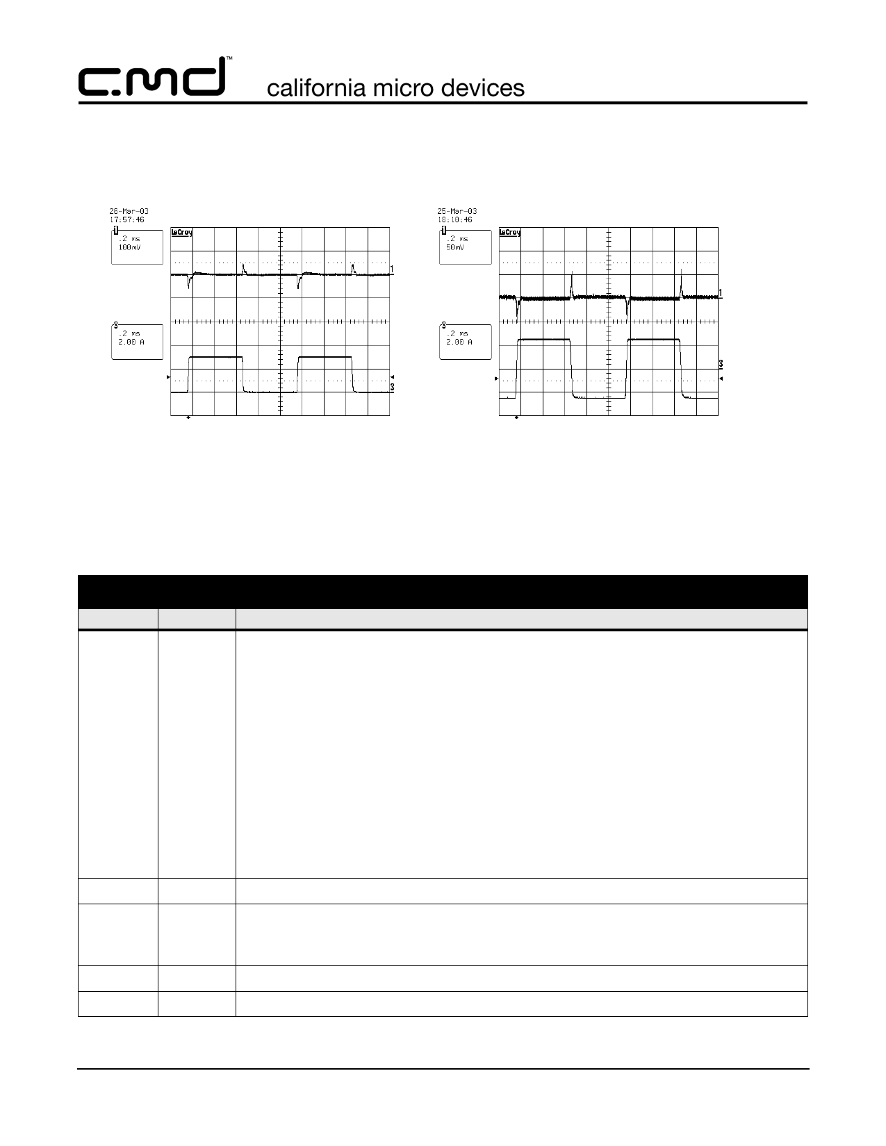
Typical Operating Characteristics
VDDQ Transient Response
PRELIMINARY
CM3205
VTT Transient Response
VDDQ
VTT
IOUT
VIN = 3.3V
IOUT Step: 10mA ~ 3A
IOUT
VIN = 3.3V
IOUT Step: -2.5A ~ +2.5A
Pin Descriptions
PIN(S)
1
2
3
4
5
NAME
PIN DESCRIPTIONS
DESCRIPTION
This pin is for VDDQ output voltage adjustment. The VDDQ output voltage is set using an
external resistor divider connected to ADJSD. The output voltage is determined by the
following formula:
VDDQ
=
1.215V × R-----1----+-----R-----2-
R1
ADJSD
VDDQ
GND
VIN
VTT
where R1 is the ground-side resistor and R2 is the upper resistor of the divider.
Connect these resistors to the VDDQ output at the point of regulation.
In addition, this input functions as a shutdown pin. Apply a voltage higher than VIN-1.2V
to this pin to simultaneously shutdown both VDDQ and VTT outputs. The outputs are
restored when the voltage on this pin falls below VIN-1.2V. A low-leakage diode in
series with the shutdown input signal is recommended to avoid interference with the
voltage adjustment setting.
VDDQ regulator output voltage pin.
GROUND reference pin. The back tab is also ground and serves as the package
heatsink. It should be soldered to the circuit board copper to remove excess heat from
the IC.
Input voltage pin, typically 3.3V from the power supply.
VTT regulator output voltage pin, which is preset to 50% of VDDQ.
© 2006 California Micro Devices Corp. All rights reserved.
05/08/06 490 N. McCarthy Blvd., Milpitas, CA 95035-5112 l Tel: 408.263.3214 l Fax: 408.263.7846 l www.cmd.com
5
Share Link: 