ATTINY40 Ver la hoja de datos (PDF) - Atmel Corporation
Número de pieza
componentes Descripción
Fabricante
ATTINY40 Datasheet PDF : 216 Pages
| |||
ATtiny40
5.2.2
5.2.3
Internal SRAM
The internal SRAM is mapped in the Data Memory space starting at address 0x0040. SRAM is
accessed from the CPU by using direct addressing, indirect addressing or via the RAM interface.
The registers R26 to R31 function as pointer register for indirect addressing. The pointer pre-
decrement and post-increment functions are also supported in connection with the indirect
addressing. Direct addressing using the LDS and STS instructions reaches only the lowest 128
locations between 0x0040 and 0x00BF. The locations beyond the first 128 bytes between
0x00C0 and 0x013F must be accessed using either indirect addressing mode (LD and ST
instructions) or via the RAM interface.
The user must pay particular attention to the RAM addressing when using the RAM interface.
The direct and indirect addressing modes use virtual RAM address, but the RAM interface uses
physical RAM address. The virtual RAM address space mapping to physical addresses is
described in Table 5-1.
For example, if the data is written to RAM using the virtual RAM address 0x0100 (instruction
STS or ST), it is mapped to physical RAM address 0x0000. Thus the physical RAM address
0x0000 must be written to the RAMAR register when the same data location is read back via the
RAM interface. On the other hand, if the same data location is read back using direct or indirect
addressing mode (instruction LDS or LD), the same virtual RAM address 0x0100 is used.
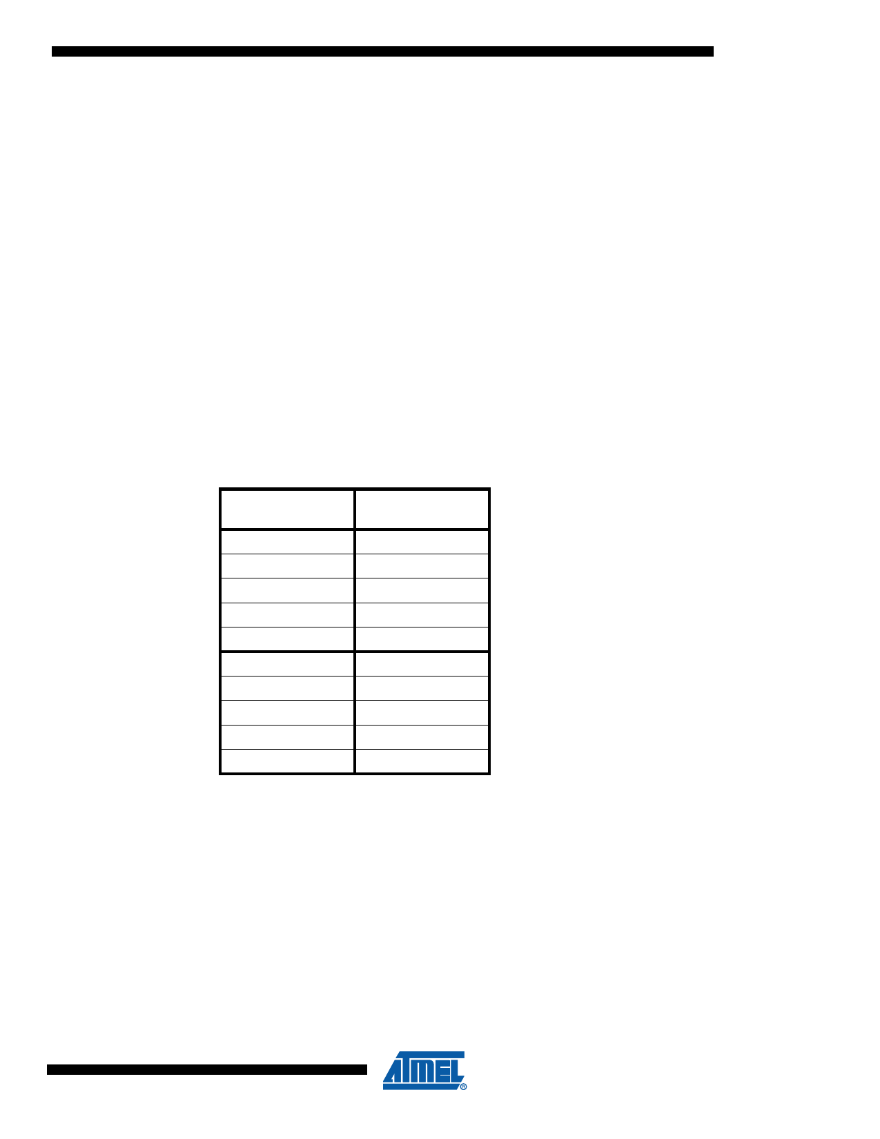
Table 5-1. SRAM Address Space
Virtual RAM
Address
Physical RAM
Address
0x0040
0x0040
–
–
–
–
–
–
0x00FF
0x00FF
0x0100
0x0000
–
–
–
–
–
–
0x013F
0x003F
RAM Interface
The RAM Interface consists of two registers, RAM Address Register (RAMAR) and RAM Data
Register (RAMDR). The registers are accessible in I/O space.
To write a location the user must first write the RAM address into RAMAR and then the data into
RAMDR. Writing the data into RAMDR triggers the write operation and the data from the source
register is written to RAM in address given by RAMAR within the same instruction cycle.
To read a location the user must first write the RAM address into RAMAR and then read the data
from RAMDR. Reading the data from RAMDR triggers the read operation and the data from
17
8263A–AVR–08/10
Share Link: 