AT89C51RB2-3CSUM Ver la hoja de datos (PDF) - Atmel Corporation
Número de pieza
componentes Descripción
Fabricante
AT89C51RB2-3CSUM Datasheet PDF : 127 Pages
| |||
AT89C51RB2/RC2
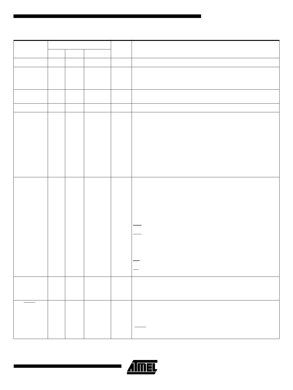
Table 12. Pin Description for 40 - 44 Pin Packages (Continued)
Pin Number
Mnemonic
DIL
LCC VQFP44 1.4 Type Name and Function
I/O CEX4: Capture/Compare External I/O for PCA Module 4
P1.0 - P1.7
I/O MOSI: SPI Master Output Slave Input line
When SPI is in master mode, MOSI outputs data to the slave peripheral. When SPI
is in slave mode, MOSI receives data from the master controller.
XTAL1
19
21
15
I
Crystal 1: Input to the inverting oscillator amplifier and input to the internal clock
generator circuits.
XTAL2
18
20
14
O Crystal 2: Output from the inverting oscillator amplifier
P2.0 - P2.7
21 - 28 24 - 31
18 - 25
I/O Port 2: Port 2 is an 8-bit bi-directional I/O port with internal pull-ups. Port 2 pins that
have 1s written to them are pulled high by the internal pull-ups and can be used as
inputs. As inputs, Port 2 pins that are externally pulled low will source current
because of the internal pull-ups. Port 2 emits the high - order address Byte during
fetches from external program memory and during accesses to external data
memory that use 16-bit addresses (MOVX @DPTR). In this application, it uses
strong internal pull-ups emitting 1s. During accesses to external data memory that
use 8-bit addresses (MOVX @Ri), port 2 emits the contents of the P2 SFR. Some
Port 2 pins receive the high order address bits during EPROM programming and
verification:
P2.0 to P2.5 for 16 KB devices
P2.0 to P2.6 for 32KB devices
P3.0 - P3.7
10 - 17 11,
13 - 19
5,
7 - 13
I/O Port 3: Port 3 is an 8-bit bi-directional I/O port with internal pull-ups. Port 3 pins that
have 1s written to them are pulled high by the internal pull-ups and can be used as
inputs. As inputs, Port 3 pins that are externally pulled low will source current
because of the internal pull-ups. Port 3 also serves the special features of the
80C51 family, as listed below.
10
11
5
I
RXD (P3.0): Serial input port
11
13
7
O TXD (P3.1): Serial output port
12
14
8
I
INT0 (P3.2): External interrupt 0
13
15
9
I
INT1 (P3.3): External interrupt 1
14
16
10
I
T0 (P3.4): Timer 0 external input
15
17
11
I
T1 (P3.5): Timer 1 external input
16
18
12
O WR (P3.6): External data memory write strobe
17
19
13
O RD (P3.7): External data memory read strobe
RST
9
10
4
Reset: A high on this pin for two machine cycles while the oscillator is running,
I/O
resets the device. An internal diffused resistor to VSS permits a power-on reset using
only an external capacitor to VCC. This pin is an output when the hardware
watchdog forces a system reset.
ALE/PROG
30
33
27
O (I) Address Latch Enable/Program Pulse: Output pulse for latching the low Byte of
the address during an access to external memory. In normal operation, ALE is
emitted at a constant rate of 1/6 (1/3 in X2 mode) the oscillator frequency, and can
be used for external timing or clocking. Note that one ALE pulse is skipped during
each access to external data memory. This pin is also the program pulse input
(PROG) during Flash programming. ALE can be disabled by setting SFR’s AUXR. 0
bit. With this bit set, ALE will be inactive during internal fetches.
11
4180E–8051–10/06
Share Link: 