AN8018SA Ver la hoja de datos (PDF) - Panasonic Corporation
Número de pieza
componentes Descripción
Fabricante
AN8018SA
Panasonic Corporation

AN8018SA Datasheet PDF : 26 Pages
| |||
AN8018SA
Voltage Regulators
s Application Notes (continued)
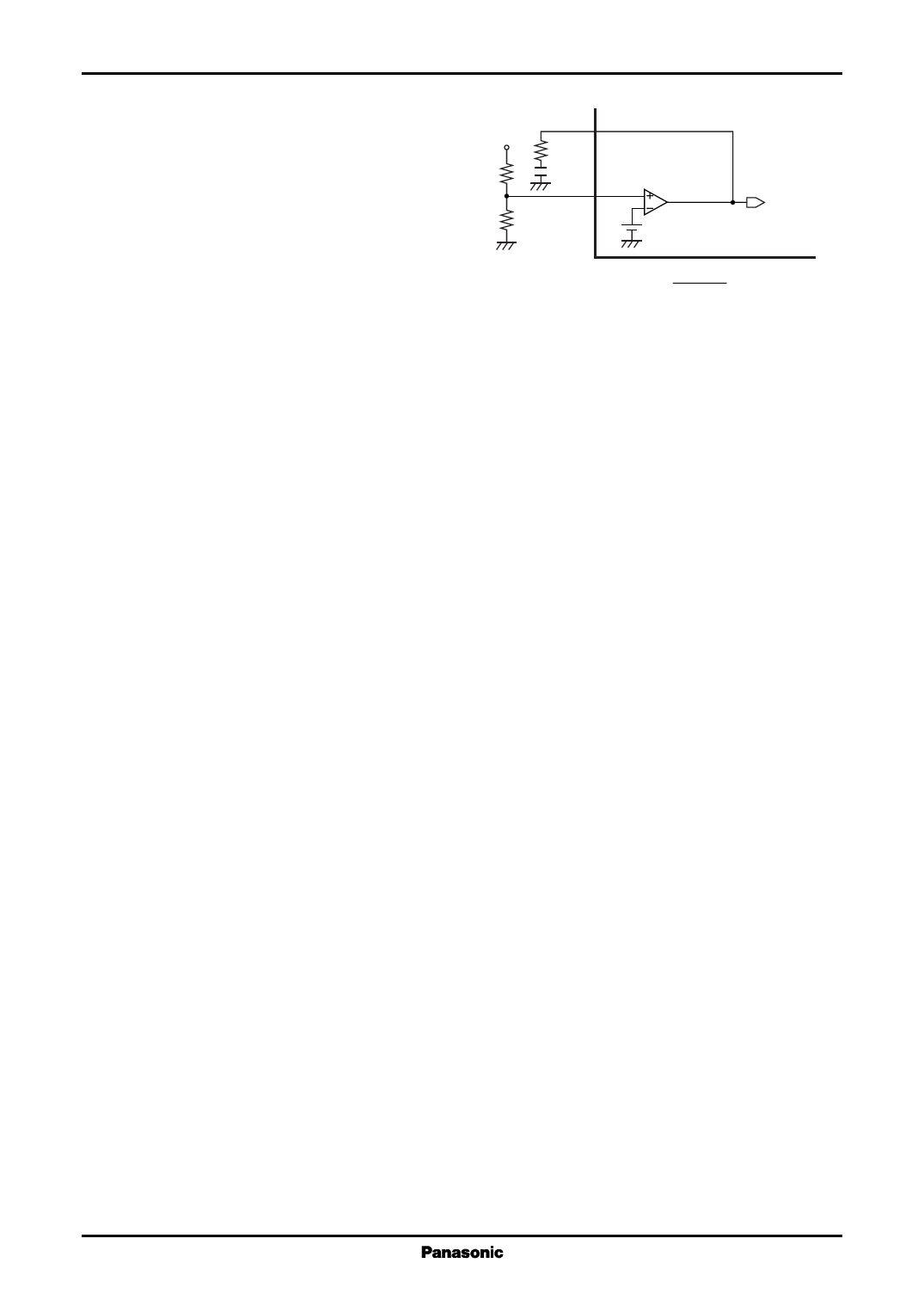
[4] Function descriptions (continued)
4. Error amplifier 2 block (continued)
Also, it is possible to perform the gain setting
and the phase compensation arbitrarily by con-
necting a resistor and a capacitor from the FB2
terminal (pin 13) to GND in series.
VOUT2
R1
R2
FB2 13
Error amplifier 2
block
14
IN+2
1.19 V
To PWM
comparator input
The output voltage VOUT2 can be set by mak-
ing connection as shown in figure 3.
VOUT2 = 1.19 ×
R1 + R2
R2
5. Timer latch short-circuit protection circuit
Figure 3. Connection method of error amplifier 2 block
(step-up output)
This circuit protects the external main switching devices, flywheel diodes, and choke coils, etc. from
destruction or deterioration if overload or short-circuit condition of power supply output lasts for a certain time.
The timer latch short-circuit protection circuit detects the output level of the error amplifier. When the output
voltage of DC-DC converter drops and the FB1 terminal (pin 5) becomes 0.9 V or more, or the FB2 terminal
(pin 13) becomes 0.22 V or less, the low-level output is given and the timer circuit is actuated to start the charge
of the external protection-enable capacitor.
If the output of the error amplifier does not return to a normal voltage range by the time when the voltage of
this capacitor reaches 1.19 V, it sets the latch circuit, and cuts off the output drive transistor, and sets the dead-time
to 100%.
6. Low input voltage malfunction prevention circuit (U.V.L.O.)
This circuit protects the system from destruction or deterioration due to control malfunction when the supply
voltage is low in the transient state of power on/off.
The low input voltage malfunction prevention circuit detects the internal reference voltage which changes
according to the supply voltage level. Until the supply voltage reaches 1.67 V during its rise time, it cuts off the
output drive transistor, and sets the dead-time to 100%. At the same time, it holds the S.C.P. terminal (pin 2) and
DT1 terminal (pin 6) to low-level, and the OSC terminal (pin 1) and DT2 terminal (pin 12) to high-level.
7. PWM comparator block
The PWM comparator controls the on-period of the output pulse according to the input voltage. The PWM1
and PWM2 block are set in an opposite logic relation of each other and on-period of each output is staggered.
The PWM1 block turns on the output transistor during the period when the triangular wave of OSC terminal
(pin 1) is lower than any lower one of the FB1 (pin 5) terminal voltage and the DT1 (pin 6) terminal voltage.
The PWM2 block turns on the output transistor during the period when the triangular wave of OSC terminal
(pin 1) is higher than any higher one of the FB2 (pin 13) terminal voltage and the DT2 (pin 12) terminal voltage.
The maximum duty ratio is variable from the outside.
Also, the soft start which gradually extends on-period of the output pulse is activated by connecting a capaci-
tor in parallel with the resistor-dividing for the maximum duty ratio setting.
8. Unlatch block
The unlatch circuit 1 block fixes the FB1 terminal (pin 5) at low level at the DT1 terminal (pin 6) is 0.20 V or
less. The unlatch circuit 2 block fixes the FB2 terminal (pin 13) at high-level at the DT2 terminal (pin 12) is 0.9
V or more. Consequently, by controlling the DT1 and the DT2 terminal voltages, it is possible to operate only one
channel or to start and stop each channel in any required sequence.
9. Output 1 block
This output circuit is open-collector type. The available output current is up to 50 mA. The breakdown voltage
of output terminal is 15 V.
10. Output 2 block
This block uses a totem pole type output circuit. By connecting the current setting resistor to the RB2 terminal,
it is possible to arbitrarily set a constant-current source-output having a small fluctuation with the supply voltage.
The available constant-current source-output is up to 50 mA.
14
Share Link: