ADP5022 Ver la hoja de datos (PDF) - Analog Devices
Número de pieza
componentes Descripción
Fabricante
ADP5022 Datasheet PDF : 28 Pages
| |||
ADP5022
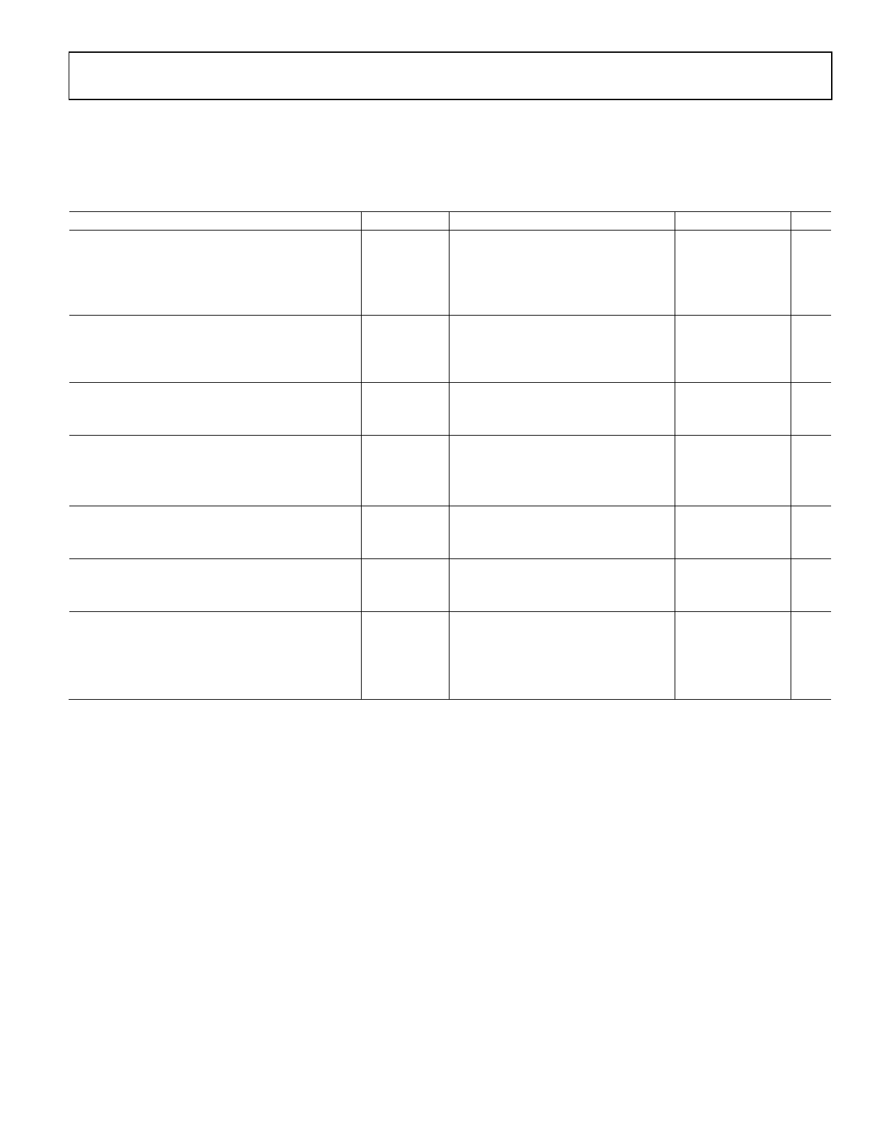
SPECIFICATIONS
VDDA = VIN1 = VIN2 = 3.6 V, VIN3 = (VOUT3 + 0.5 V) or 2.4 V, whichever is greater, VIN3 ≤ VIN1, TJ = −40°C to +125°C, unless
otherwise noted.1
Table 1.
Parameter
INPUT VOLTAGE RANGE
System and Buck Input Supplies Voltage Range
LDO Input Supply Voltage Range
SHUTDOWN CURRENT
THERMAL SHUTDOWN
Thermal Shutdown Threshold
Thermal Shutdown Hysteresis
EN1, EN2, EN3, MODE INPUTS
EN1, EN2, EN3, MODE Input Logic High
EN1, EN2, EN3, MODE Input Logic Low
EN1, EN2, EN3, MODE Input Leakage Current
STANDBY CURRENT
All Channels Enabled, No Load
All Channels Enabled, No Load, No Buck Switching
VIN3 UNDERVOLTAGE LOCKOUT
Input Voltage Rising
Input Voltage Falling
VDDA UNDERVOLTAGE LOCKOUT
Input Voltage Rising
Input Voltage Falling
Symbol
VDDA, VIN1,
and VIN2
VIN3
IGND-SD
TSDTH
TSDHYS
VIH
VIL
VI-LEAKAGE
ISTBY
ISTBY-NOSW
UVLOVIN3RISE
UVLOVIN3FALL
UVLOVDDARISE
UVLOVDDAFALL
Test Conditions/Comments
Min Typ Max Unit
Low UVLO level models
High UVLO level models
2.4
5.5 V
4.5
5.5 V
2.3
5.5 V
EN1 = EN2 = EN3 = GND
EN1 = EN2 = EN3 = GND
TJ = −40°C to +85°C
0.5
μA
2 μA
TJ rising
150
°C
20
°C
VDDA = VIN1 = VIN2
VDDA = VIN1 = VIN2
Pin at (VDDA = VIN1 = VIN2) or GND
1.2
V
0.4 V
0.05 1 μA
80
μA
59 85 μA
2.20 V
1.45
V
High UVLO level (factory programmed)
Low UVLO level (factory programmed)
High UVLO level (factory programmed) 3.40
Low UVLO level (factory programmed) 2.00
4.15 V
2.35 V
V
V
1 All limits at temperature extremes are guaranteed via correlation using standard statistical quality control.
Rev. C | Page 3 of 28
Share Link: 