ADP5022 Ver la hoja de datos (PDF) - Analog Devices
Número de pieza
componentes Descripción
Fabricante
ADP5022 Datasheet PDF : 28 Pages
| |||
Dual 3 MHz, 600 mA Buck
Regulator with 150 mA LDO
ADP5022
FEATURES
Input voltage range: 2.4 V to 5.5 V
Tiny 16-ball, 2 mm × 2 mm WLCSP package
Overcurrent and thermal protection
Soft start
Factory programmable undervoltage lockout on VDDA
system supply of either 2.2 V or 3.9 V
Factory programmable default output voltages for all
3 channels
Buck1 and Buck2 key specifications
Current mode architecture for excellent transient response
3 MHz operating frequency
Uses tiny multilayer inductors and capacitors
Forced PWM and auto PWM/PSM modes
Out-of-phase operation for reduced input filtering
100% duty cycle low dropout mode
24 μA typical quiescent current per channel, no switching
LDO key specifications
Stable with 1 μF ceramic output capacitors
High PSRR
60 dB up to 10 KHz
Low output noise
65 μV rms output noise at VOUT3 = 3.3 V
Low dropout voltage: 150 mV @ 150 mA load
11 μA typical ground current at no load
APPLICATIONS
USB devices
Handheld products
Multivoltage power for processors, ASICS, FPGAs,
and RF chipsets
GENERAL DESCRIPTION
The ADP5022 is a micro power management unit (micro PMU)
that combines two high performance buck regulators and a low
dropout regulator (LDO) in a tiny 16-ball 2.08 mm × 2.08 mm
WLCSP to meet demanding performance and board space
requirements.
The high switching frequency of the buck regulators enables
tiny multilayer external components and minimizes the board
space required. When the MODE pin is set high, the buck reg-
ulators operate in forced PWM mode. When the MODE pin is
set low, the buck regulators automatically switch operating
modes, depending on the load current level. At higher output
loads, the buck regulators operate in PWM mode. When the
load current falls below a predefined threshold, the regulators
operate in power save mode (PSM), improving the light-load
efficiency.
The two bucks operate out-of-phase to reduce the input
capacitor requirement and noise.
The low quiescent current, low dropout voltage, and wide input
voltage range of the ADP5022 LDO extends the battery life of
portable devices. The LDO maintains power supply rejection
greater than 60 dB for frequencies as high as 10 kHz while
operating with a low headroom voltage.
Each regulator in the ADP5022 has a dedicated, independent
enable pin. A high voltage level applied to the enable pin activates
the respective regulator. The default output voltages are factory
programmable and can be set to a wide range of options.
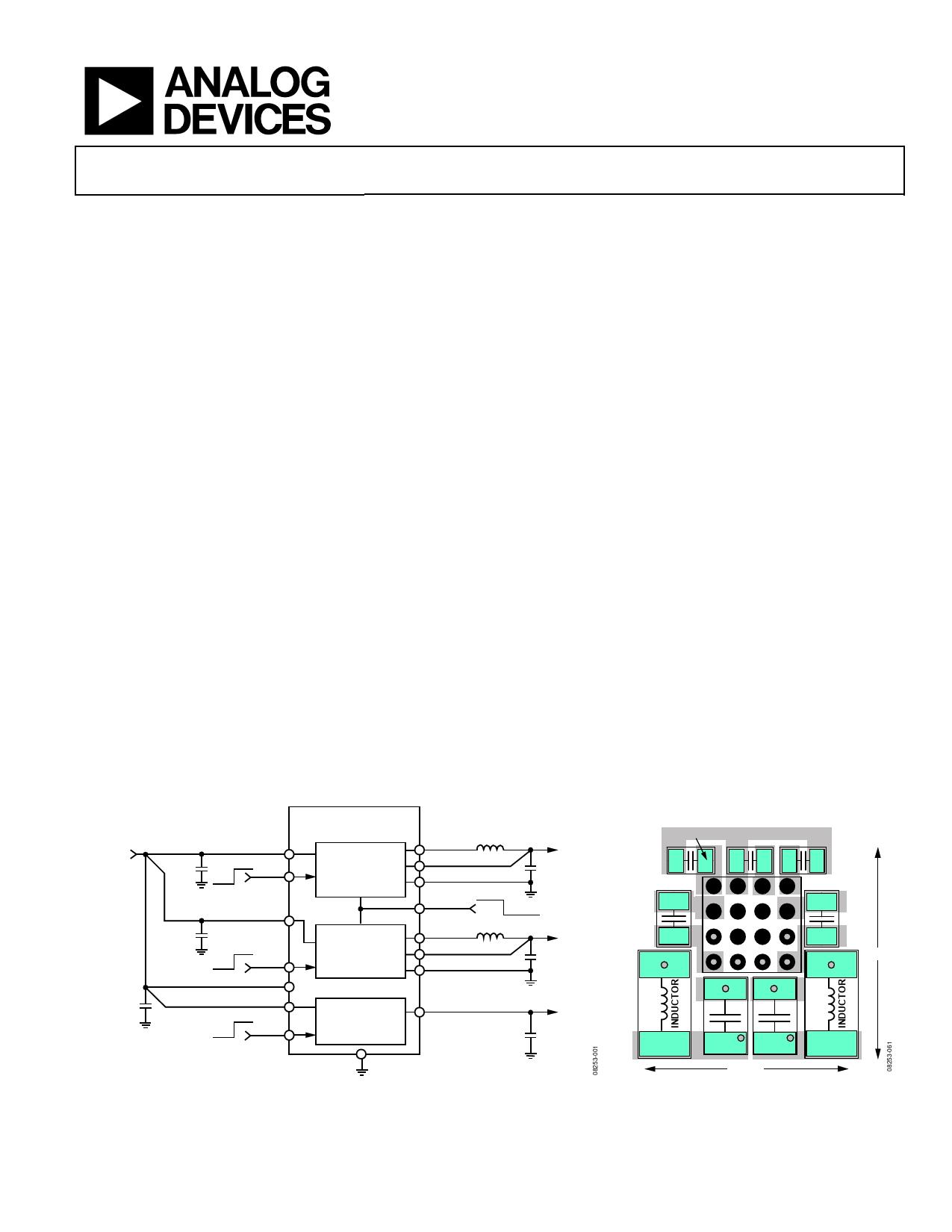
VIN = 2.4V
TO 5.5V
C1
1µF
C2
4.7µF
C3
4.7µF
ADP5022
ON
OFF
VIN1
EN1
VIN2
ON
OFF
EN2
VDDA
ON
OFF
VIN3
EN3
BUCK1
EN_BK1
MODE
MODE
BUCK2
EN_BK2
LDO1
EN_LDO1
SW1
VOUT1
PGND1
MODE
SW2
VOUT2
PGND2
VOUT3
AGND
Figure 1. Typical Applications Circuit
L1
1µH
VOUT1 @
C4 600mA
10µF
PWM
L2 PWM/PSM
1µH
VOUT2 @
C5 600mA
10µF
VOUT3 @
150mA
C6
1µF
COUT_3
C1
C3
C4
C2
5.0mm
L1
COUT_1 COUT_2
4.7mm
Figure 2. Typical PCB Layout
Rev. C
Information furnished by Analog Devices is believed to be accurate and reliable. However, no
responsibility is assumed by Analog Devices for its use, nor for any infringements of patents or other
rights of third parties that may result from its use. Specifications subject to change without notice. No
license is granted by implication or otherwise under any patent or patent rights of Analog Devices.
Trademarks and registered trademarks are the property of their respective owners.
One Technology Way, P.O. Box 9106, Norwood, MA 02062-9106, U.S.A.
Tel: 781.329.4700
www.analog.com
Fax: 781.461.3113 ©2009–2010 Analog Devices, Inc. All rights reserved.
Share Link: 