ADE7769 Ver la hoja de datos (PDF) - Analog Devices
Número de pieza
componentes Descripción
Fabricante
ADE7769 Datasheet PDF : 20 Pages
| |||
( ) ∞
i(t) = IO + 2 × ∑ Ih × sin hωt + βh
(3)
h≠o
where:
i(t) is the instantaneous current.
I0 is the dc component.
Ih is the rms value of current harmonic h.
βh is the phase angle of the current harmonic.
Using Equations 2 and 3, the real power (P) can be expressed in
terms of its fundamental real power (P1) and harmonic real
power (PH) as P = P1 + PH
where:
P1 = V1 × I1 cos φ 1
(4)
φ1 = α1 − β1
and
∞
PH = ∑Vh × Ih cos φh
(5)
h≠1
φh = αh − βh
In Equation 5, a harmonic real power component is generated
for every harmonic, provided that harmonic is present in both
the voltage and current waveforms. The power factor calcu-
lation has previously been shown to be accurate in the case of a
pure sinusoid. Therefore, the harmonic real power must also
correctly account for the power factor because it is made up of
a series of pure sinusoids.
Note that the input bandwidth of the analog inputs is 7 kHz at
the nominal internal oscillator frequency of 450 kHz.
ANALOG INPUTS
Channel V1 (Current Channel)
The voltage output from the current sensor is connected to the
ADE7769 here. Channel V1 is a fully differential voltage input.
V1P is the positive input with respect to V1N.
The maximum peak differential signal on Channel V1 should
be less than ±30 mV (21 mV rms for a pure sinusoidal signal)
for specified operation.
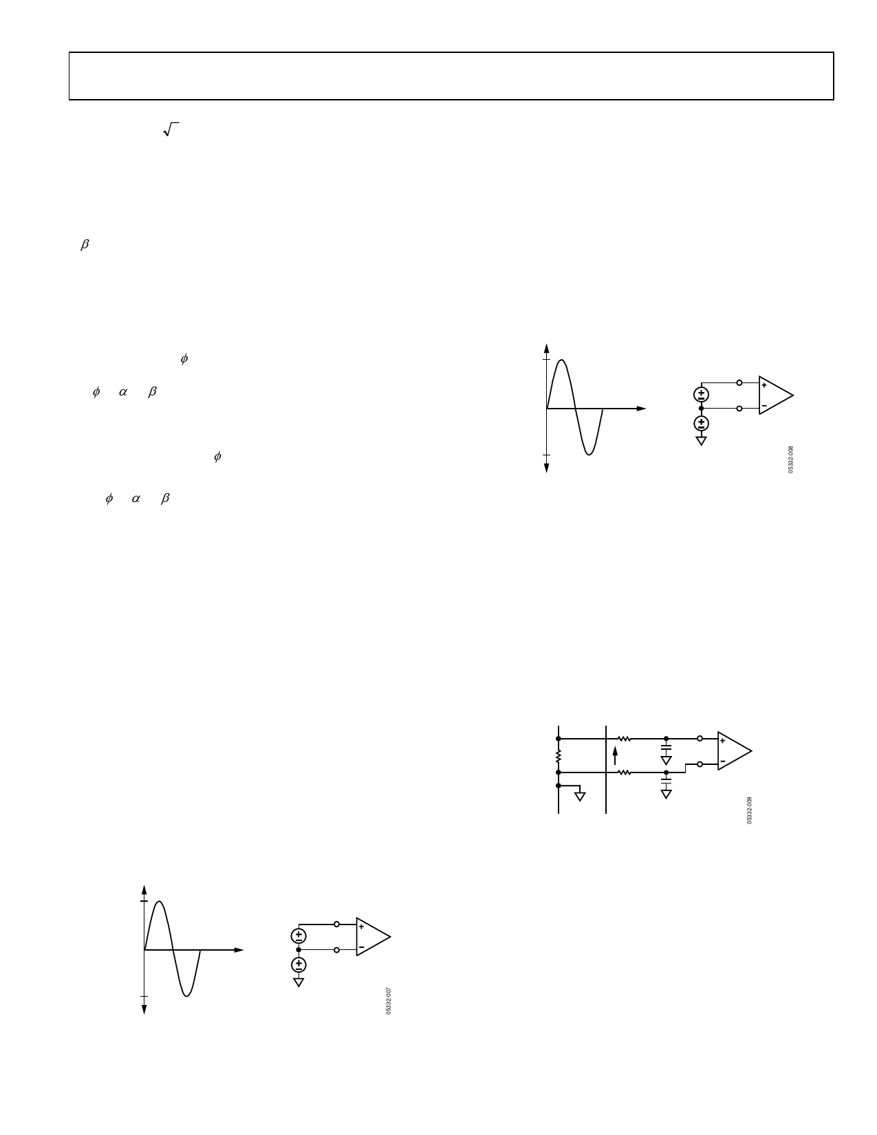
V1
+30mV
VCM
DIFFERENTIAL INPUT
±30mV MAX PEAK
COMMON-MODE
±6.25mV MAX
V1P
V1 V1N
VCM
–30mV
AGND
Figure 17. Maximum Signal Levels, Channel V1
ADE7769
Figure 17 shows the maximum signal levels on V1P and V1N.
The maximum differential voltage is ±30 mV. The differential
voltage signal on the inputs must be referenced to a common
mode, for example, AGND. The maximum common-mode
signal is ±6.25 mV, as shown in Figure 17.
Channel V2 (Voltage Channel)
The output of the line voltage sensor is connected to the
ADE7769 at this analog input. Channel V2 is a fully differential
voltage input with a maximum peak differential signal of
±165 mV. Figure 18 shows the maximum signal levels that can
be connected to the ADE7769 Channel V2.
V2
+165mV
VCM
DIFFERENTIAL INPUT
±165mV MAX PEAK
COMMON-MODE
±25mV MAX
V2P
V2 V2N
VCM
–165mV
AGND
Figure 18. Maximum Signal Levels, Channel V2
Channel V2 is usually driven from a common-mode voltage,
that is, the differential voltage signal on the input is referenced
to a common mode (usually AGND). The analog inputs of the
ADE7769 can be driven with common-mode voltages of up to
25 mV with respect to AGND. However, best results are
achieved using a common mode equal to AGND.
Typical Connection Diagrams
Figure 19 shows a typical connection diagram for Channel V1.
A shunt is the current sensor selected for this example because
of its low cost compared to other current sensors, such as the
current transformer (CT). This IC is ideal for low current meters.
SHUNT
RF
±30mV
V1P
CF
V1N
RF
CF
AGND
PHASE NEUTRAL
Figure 19. Typical Connection for Channel V1
Figure 20 shows a typical connection for Channel V2. Typically,
the ADE7769 is biased around the phase wire, and a resistor
divider is used to provide a voltage signal that is proportional to
the line voltage. Adjusting the ratio of RA, RB,B and RF is also a
convenient way of carrying out a gain calibration on a meter.
Rev. A | Page 11 of 20
Share Link: 