AD9250(Rev0) Ver la hoja de datos (PDF) - Analog Devices
Número de pieza
componentes Descripción
Fabricante
AD9250
(Rev.:Rev0)
(Rev.:Rev0)
Analog Devices

AD9250 Datasheet PDF : 44 Pages
| |||
AD9250
Data Sheet
Nyquist Clock Input Options
The AD9250 Nyquist clock input supports a differential clock
between 40 MHz to 625 MHz. The clock input structure supports
differential input voltages from 0.3 V to 3.6 V and is therefore
compatible with various logic family inputs, such as CMOS,
LVDS, and LVPECL. A sine wave input is also accepted, but
higher slew rates typically provide optimal performance. Clock
source jitter is a critical parameter that can affect performance, as
described in the Jitter Considerations section. If the inputs are
floated, pull the CLK− pin low to prevent spurious clocking.
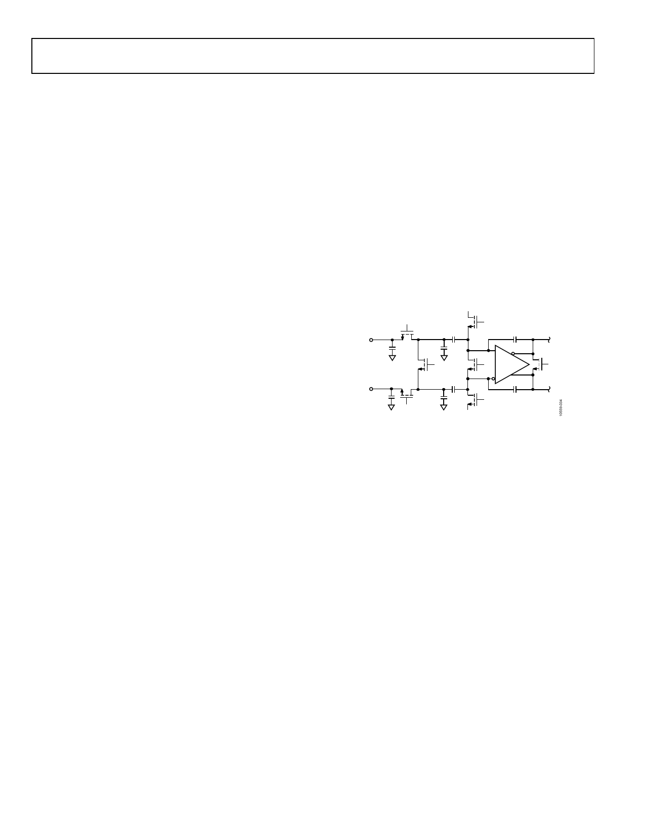
The Nyquist clock input pins, CLK+ and CLK−, are internally
biased to 0.9 V and have a typical input impedance of 4 pF in
parallel with 10 kΩ (see Figure 39). The input clock is typically
ac-coupled to CLK+ and CLK−. Some typical clock drive circuits
are presented in Figure 40 through Figure 43 for reference.
AVDD
CLK+
4pF
0.9V
CLK–
4pF
as the AD9510, AD9511, AD9512, AD9513, AD9514, AD9515,
AD9516, AD9517, AD9518, AD9520, AD9522, AD9523, AD9524,
and ADCLK905, ADCLK907, and ADCLK925.
CLOCK
INPUT
CLOCK
INPUT
50kΩ
0.1µF
AD95xx
0.1µF PECL DRIVER
50kΩ
240Ω
0.1µF
ADC
CLK+
0.1µF
240Ω
100Ω
CLK–
Figure 42. Differential PECL Sample Clock (Up to 625 MHz)
Analog Devices also offers LVDS clock drivers with excellent jitter
performance. A typical circuit is shown in Figure 43 and uses
LVDS drivers such as the AD9510, AD9511, AD9512, AD9513,
AD9514, AD9515, AD9516, AD9517, AD9518, AD9520, AD9522,
AD9523, and AD9524.
CLOCK
INPUT
CLOCK
INPUT
50kΩ
0.1µF
AD95xx
0.1µF LVDS DRIVER
50kΩ
0.1µF
100Ω
0.1µF
ADC
CLK+
CLK–
Figure 39. Equivalent Nyquist Clock Input Circuit
For applications where a single-ended low jitter clock between
40 MHz to 200 MHz is available, an RF transformer is
recommended. An example using an RF transformer in the clock
network is shown in Figure 40. At frequencies above 200 MHz,
an RF balun is recommended, as seen in Figure 41. The back-to-
back Schottky diodes across the transformer secondary limit
clock excursions into the AD9250 to approximately 0.8 V p-p
differential. This limit helps prevent the large voltage swings of
the clock from feeding through to other portions of the AD9250,
yet preserves the fast rise and fall times of the clock, which are
critical to low jitter performance.
Figure 43. Differential LVDS Sample Clock (Up to 625 MHz)
RF Clock Input Options
The AD9250 RF clock input supports a single-ended clock
between 625 GHz to 1.5 GHz. The equivalent RF clock input
circuit is shown in Figure 44. The input is self biased to 0.9 V and is
typically ac-coupled. The input has a typical input impedance of
10 kΩ in parallel with 1 pF at the RFCLK pin.
0.5pF
RFCLK
10kΩ
BIAS
CONTROL
INTERNAL
CLOCK DRIVER
CLOCK
INPUT
390pF
Mini-Circuits®
ADT1-1WT, 1:1Z
XFMR 390pF
50Ω 100Ω
390pF
SCHOTTKY
DIODES:
HSMS2822
ADC
CLK+
CLK–
Figure 40. Transformer-Coupled Differential Clock (Up to 200 MHz)
390pF
CLOCK
INPUT
25Ω
390pF
ADC
CLK+
390pF
1nF
CLK–
25Ω
SCHOTTKY
DIODES:
HSMS2822
Figure 41. Balun-Coupled Differential Clock (Up to 625 MHz)
In some cases, it is desirable to buffer or generate multiple
clocks from a single source. In those cases, Analog Devices, Inc.,
offers clock drivers with excellent jitter performance. Figure 42
shows a typical PECL driver circuit that uses PECL drivers such
Figure 44. Equivalent RF Clock Input Circuit
It is recommended to drive the RF clock input of the AD9250
with a PECL or sine wave signal with a minimum signal amplitude
of 600 mV peak to peak. Regardless of the type of signal being
used, clock source jitter is of the most concern, as described in the
Jitter Considerations section. Figure 45 shows the preferred method
of clocking when using the RF clock input on the AD9250. It is
recommended to use a 50 Ω transmission line to route the clock
signal to the RF clock input of the AD9250 due to the high
frequency nature of the signal and terminate the transmission
line close to the RF clock input.
ADC
50Ω Tx LINE
RF CLOCK
INPUT
0.1µF
50Ω
RFCLK
Figure 45. Typical RF Clock Input Circuit
Rev. 0 | Page 20 of 44
Share Link: