AD7755 Ver la hoja de datos (PDF) - Analog Devices
Número de pieza
componentes Descripción
Fabricante
AD7755 Datasheet PDF : 16 Pages
| |||
AD7755
Using Equations 1 and 2, the real power P can be expressed in
terms of its fundamental real power (P1) and harmonic real
power (PH).
P = P1 + PH
where:
P1 = V1 × I1 cos φ1
(3)
φ1 = α1 – β1
and
∝
PH = ∑Vh × Ih cos φh
h ≠1
(4)
φh = αh – βh
As can be seen from Equation 4 above, a harmonic real power
component is generated for every harmonic, provided that har-
monic is present in both the voltage and current waveforms.
The power factor calculation has previously been shown to be
accurate in the case of a pure sinusoid, therefore the harmonic
real power must also correctly account for power factor since it
is made up of a series of pure sinusoids.
Note that the input bandwidth of the analog inputs is 14 kHz
with a master clock frequency of 3.5795 MHz.
Table I. Gain Selection for Channel 1
Maximum
G1
G0
Gain
Differential Signal
0
0
1
0
1
2
1
0
8
1
1
16
± 470 mV
± 235 mV
± 60 mV
± 30 mV
Channel V2 (Voltage Channel )
The output of the line voltage transducer is connected to the
AD7755 at this analog input. Channel V2 is a fully differential
voltage input. The maximum peak differential signal on Chan-
nel 2 is ± 660 mV. Figure 23 illustrates the maximum signal
levels that can be connected to the AD7755 Channel 2.
V2
+660mV
VCM
–660mV
DIFFERENTIAL INPUT
؎660mV MAX PEAK
V2P
V2 V2N
COMMON-MODE
؎100mV MAX
VCM
AGND
ANALOG INPUTS
Channel V1 (Current Channel )
The voltage output from the current transducer is connected to
the AD7755 here. Channel V1 is a fully differential voltage
input. V1P is the positive input with respect to V1N.
The maximum peak differential signal on Channel 1 should be
less than ± 470 mV (330 mV rms for a pure sinusoidal signal) for
specified operation. Note that Channel 1 has a programmable
gain amplifier (PGA) with user selectable gain of 1, 2, 8 or 16
(see Table I). These gains facilitate easy transducer interfacing.
V1
+470mV
VCM
–470mV
DIFFERENTIAL INPUT
؎470mV MAX PEAK
COMMON-MODE
؎100mV MAX
V1P
V1 V1N
VCM
AGND
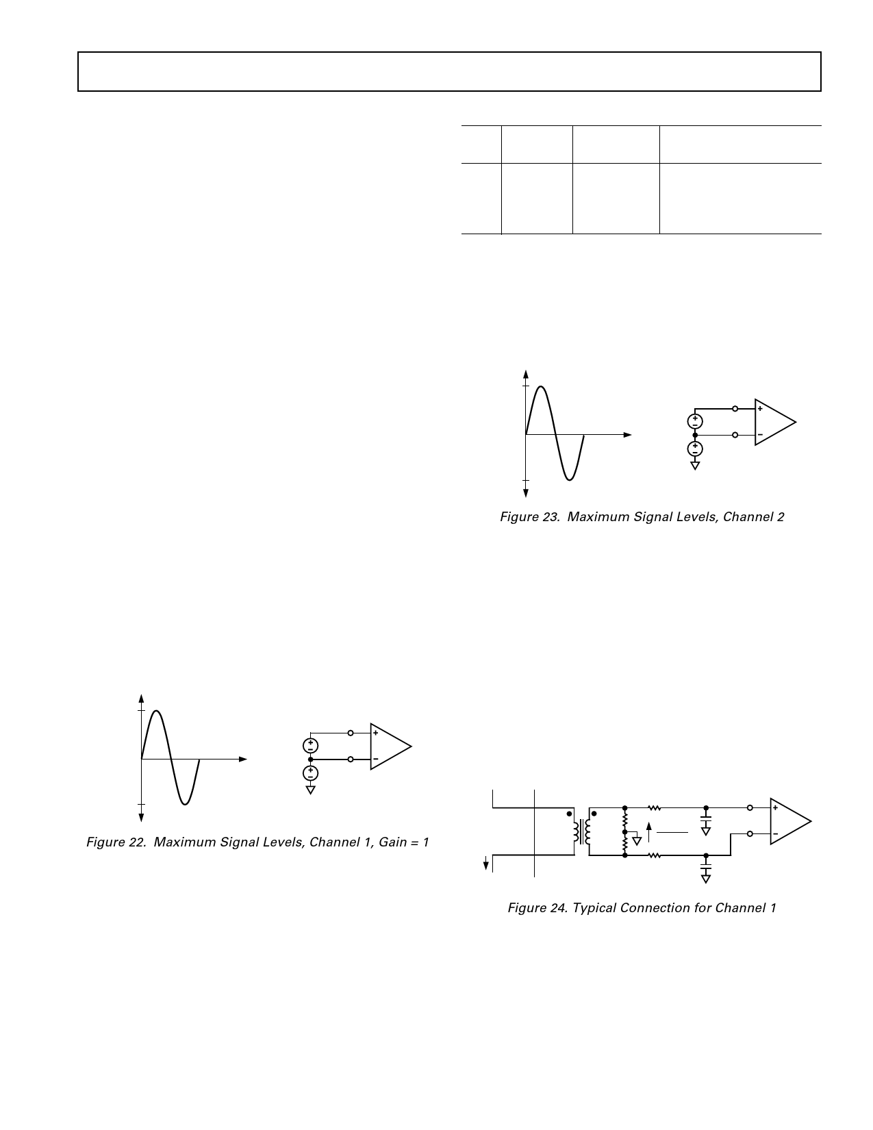
Figure 22. Maximum Signal Levels, Channel 1, Gain = 1
The diagram in Figure 22 illustrates the maximum signal levels
on V1P and V1N. The maximum differential voltage is ±470 mV
divided by the gain selection. The differential voltage signal on
the inputs must be referenced to a common mode, e.g. AGND.
The maximum common mode signal is ± 100 mV as shown in
Figure 22.
Figure 23. Maximum Signal Levels, Channel 2
Channel 2 must be driven from a common-mode voltage, i.e.,
the differential voltage signal on the input must be referenced to
a common mode (usually AGND). The analog inputs of the
AD7755 can be driven with common-mode voltages of up to
100 mV with respect to AGND. However best results are
achieved using a common mode equal to AGND.
Typical Connection Diagrams
Figure 24 shows a typical connection diagram for Channel V1.
A CT (current transformer) is the current transducer selected for
this example. Notice the common-mode voltage for Channel 1
is AGND and is derived by center tapping the burden resistor
to AGND. This provides the complementary analog input sig-
nals for V1P and V1N. The CT turns ratio and burden resistor
Rb are selected to give a peak differential voltage of ± 470 mV/
Gain at maximum load.
CT
Rb
Rf
؎470mV
GAIN
V1P
Cf
V1N
IP
AGND
PHASE NEUTRAL
Rf
Cf
Figure 24. Typical Connection for Channel 1
REV. B
–11–
Share Link: 