A40MX02(2014) Ver la hoja de datos (PDF) - Microsemi Corporation
Número de pieza
componentes Descripción
Fabricante
A40MX02 Datasheet PDF : 143 Pages
| |||
40MX and 42MX FPGA Families
MultiPlex I/O Modules
42MX devices feature Multiplex I/Os and support 5.0V, 3.3V, and mixed 3.3V/5.0V operations.
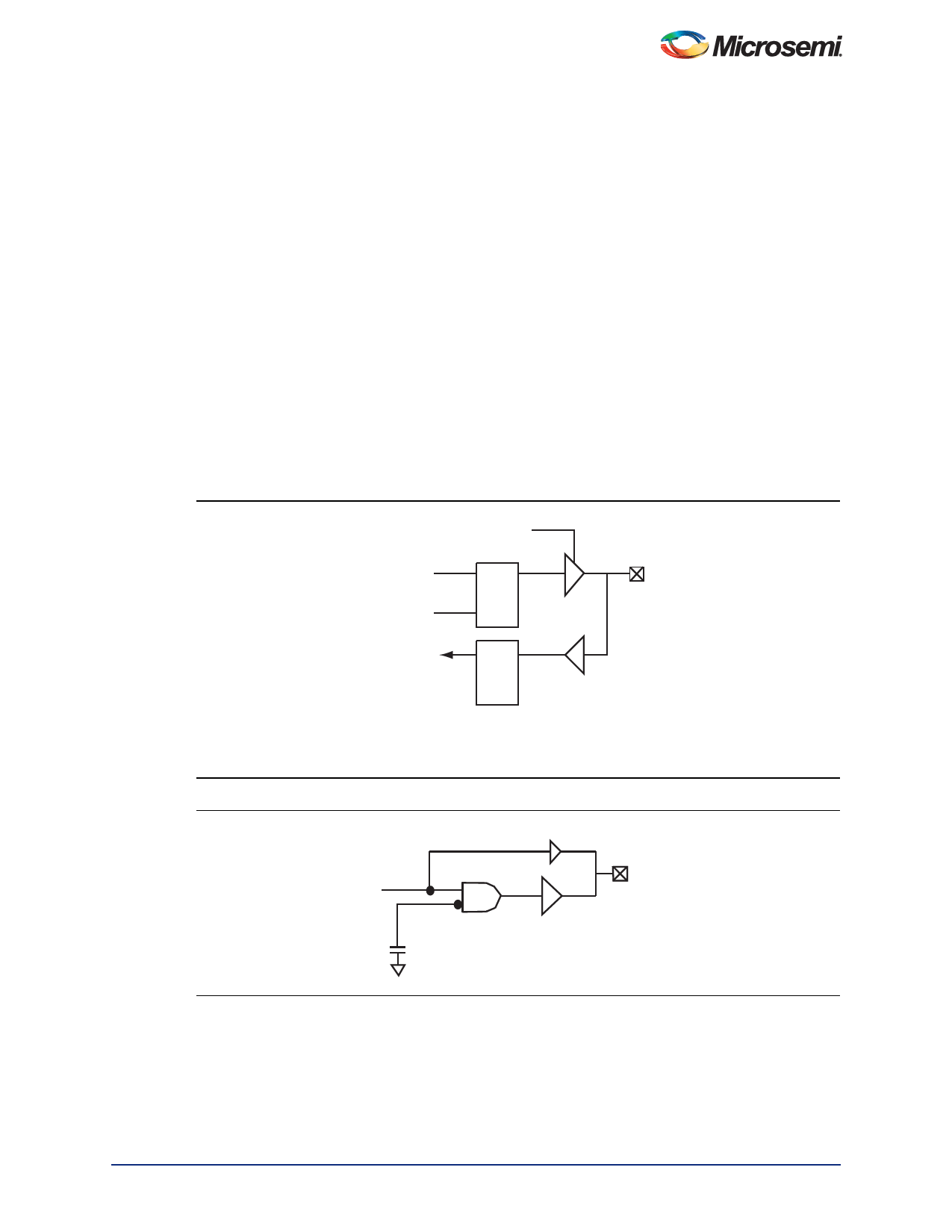
The MultiPlex I/O modules provide the interface between the device pins and the logic array. Figure 1-9 is a block
diagram of the 42MX I/O module. A variety of user functions, determined by a library macro selection, can be
implemented in the module. (Refer to the Antifuse Macro Library Guide for more information.) All 42MX I/O modules
contain tristate buffers, with input and output latches that can be configured for input, output, or bidirectional operation.
All 42MX devices contain flexible I/O structures, where each output pin has a dedicated output-enable control
(Figure 1-9). The I/O module can be used to latch input or output data, or both, providing fast set-up time. In addition,
the Designer software tools can build a D-type flip-flop using a C-module combined with an I/O module to register input
and output signals. Refer to the Antifuse Macro Library Guide for more details.
A42MX24 and A42MX36 devices also offer selectable PCI output drives, enabling 100% compliance with version 2.1
of the PCI specification. For low-power systems, all inputs and outputs are turned off to reduce current consumption to
below 500A.
To achieve 5.0V or 3.3V PCI-compliant output drives on A42MX24 and A42MX36 devices, a chip-wide PCI fuse is
programmed via the Device Selection Wizard in the Designer software (Figure 1-10). When the PCI fuse is not
programmed, the output drive is standard.
Designer software development tools provide a design library of I/O macro functions that can implement all I/O
configurations supported by the MX FPGAs.
EN
QD
From Array
PAD
G/CLK*
To Array
QD
G/CLK*
Note: *Can be configured as a Latch or D Flip-Flop (Using C-Module)
Figure 1-9 • 42MX I/O Module
STD
Signal
PCI Enable
Fuse
PCI
Drive
Output
Figure 1-10 • PCI Output Structure of A42MX24 and A42MX36 Devices
1-7
Revision 12
Share Link: 