A40MX02(2014) Ver la hoja de datos (PDF) - Microsemi Corporation
Número de pieza
componentes Descripción
Fabricante
A40MX02 Datasheet PDF : 143 Pages
| |||
40MX and 42MX FPGA Families
Power Supply
MX devices are designed to operate in both 5.0V and 3.3V environments. In particular, 42MX devices can operate in
mixed 5.0 V/3.3 V systems. Table 1-1 describes the voltage support of MX devices.
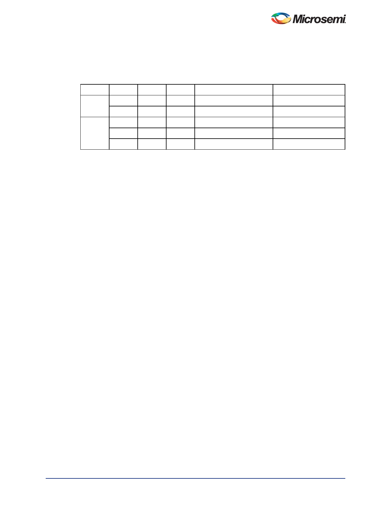
Table 1-1 • Voltage Support of MX Devices
Device
VCC
VCCA
VCCI
Maximum Input Tolerance
Nominal Output Voltage
40MX
5.0 V
–
–
5.5 V
5.0 V
3.3 V
–
–
3.6 V
3.3 V
42MX
–
5.0 V
5.0 V
5.5 V
5.0 V
–
3.3 V
3.3 V
3.6 V
3.3 V
–
5.0 V
3.3 V
5.5 V
3.3 V
For A42MX24 and A42MX36 devices the VCCA supply has to be monotonic during power up in order for the POR to
issue reset to the JTAG state machine correctly. For more information, refer to MX_PowerUp_AN, (AC291).
Power-Up/Down in Mixed-Voltage Mode
When powering up 42MX in mixed voltage mode (VCCA = 5.0 V and VCCI = 3.3 V), VCCA must be greater than or
equal to VCCI throughout the power-up sequence. If VCCI exceeds VCCA during
power-up, one of two things will happen:
• The input protection diode on the I/Os will be forward biased
• The I/Os will be at logical High
In either case, ICC rises to high levels.
For power-down, any sequence with VCCA and VCCI can be implemented.
Transient Current
Due to the simultaneous random logic switching activity during power-up, a transient current may appear on the core
supply (VCC). Customers must use a regulator for the VCC supply that can source a minimum of 100 mA for transient
current during power-up. Failure to provide enough power can prevent the system from powering up properly and
result in functional failure. However, there are no reliability concerns, since transient current is distributed across the
die instead of confined to a localized spot.
Since the transient current is not due to I/O switching, its value and duration are independent of the VCCI.
Low Power Mode
42MX devices have been designed with a Low Power Mode. This feature, activated with setting the special LP pin to
HIGH for a period longer than 800 ns, is particularly useful for battery-operated systems where battery life is a primary
concern. In this mode, the core of the device is turned off and the device consumes minimal power with low standby
current. In addition, all input buffers are turned off, and all outputs and bidirectional buffers are tristated. Since the core
of the device is turned off, the states of the registers are lost. The device must be re-initialized when exiting Low Power
Mode. I/Os can be driven during LP mode, and clock pins should be driven HIGH or LOW and should not float to avoid
drawing current. To exit LP mode, the LP pin must be pulled LOW for over 200 µs to allow for charge pumps to power
up, and device initialization will begin.
1-9
Revision 12
Share Link: 