A28F200BX-B Ver la hoja de datos (PDF) - Intel
Número de pieza
componentes Descripción
Fabricante
A28F200BX-B Datasheet PDF : 33 Pages
| |||
A28F200BX-T B
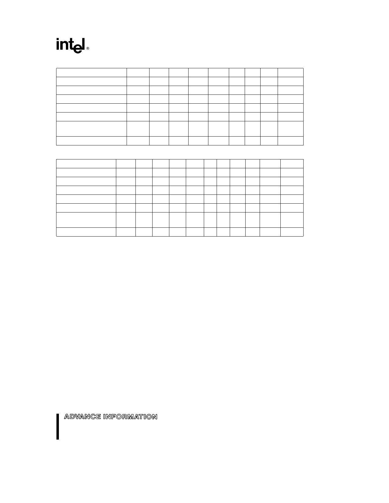
Table 1 Bus Operations for WORD-WIDE Mode (BYTE e VIH)
Mode
Notes RP
CE
OE
WE
A9 A0 VPP DQ0–15
Read
1 2 3 VIH
VIL
VIL
VIH
X
X
X DOUT
Output Disable
VIH
VIL
VIH
VIH
X
X
X High Z
Standby
VIH
VIH
X
X
X
X
X High Z
Deep Power-Down
9
VIL
X
X
X
X
X
X High Z
Intelligent Identifier (Mfr)
4
VIH
VIL
VIL
VIH VID VIL X 0089H
Intelligent Identifier (Device) 4 5
VIH
VIL
VIL
VIH VID VIH X 2274H
2275H
Write
6 7 8 VIH
VIL
VIH
VIL
X
X
X DIN
Table 2 Bus Operations for BYTE-WIDE Mode (BYTE e VIL)
Mode
Notes RP CE OE WE A9 A0 Ab1 VPP
Read
1 2 3 VIH VIL VIL VIH X X
X
X
Output Disable
VIH VIL VIH VIH X X
X
X
Standby
VIH VIH
X
X XX X X
Deep Power-Down
9
VIL
X
X
X XX X X
Intelligent Identifier (Mfr) 4
VIH VIL VIL VIH VID VIL X
X
Intelligent Identifier
(Device)
4 5 VIH VIL VIL VIH VID VIH X
X
DQ0 – 7
DOUT
High Z
High Z
High Z
89H
74H
75H
DQ8 – 14
High Z
High Z
High Z
High Z
High Z
High Z
Write
6 7 8 VIH VIL VIH VIL X X
X
X DIN
High Z
NOTES
1 Refer to DC Characteristics
2 X can be VIL or VIH for control pins and addresses VPPL or VPPH for VPP
3 See DC characteristics for VPPL VPPH VHH VID voltages
4 Manufacturer and Device codes may also be accessed via a CUI write sequence A1 – A17 e X
5 Device ID e 2274H for A28F200BX-T and 2275H for A28F200BX-B
6 Refer to Table 3 for valid DIN during a write operation
7 Command writes for Block Erase or Word Byte Write are only executed when VPP e VPPH
8 To write or erase the boot block hold RP at VHH
9 RP must be at GND g0 2V to meet the 80 mA maximum deep power-down current
3 2 Read Operations
The 2-Mbit boot block flash family has three user
read modes Array Intelligent Identifier and Status
Register Status Register read mode will be dis-
cussed in detail in the ‘‘Write Operations’’ section
During power-up conditions (VCC supply ramping) it
takes a maximum of 300 ns from when VCC is at
4 5V minimum to valid data on the outputs
3 2 1 READ ARRAY
If the memory is not in the Read Array mode it is
necessary to write the appropriate read mode com-
mand to the CUI The 2-Mbit boot block flash family
has three control functions all of which must be logi-
cally active to obtain data at the outputs Chip-En-
able CE is the device selection control Reset
Power-Down RP is the device power control Out-
put-Enable OE is the DATA INPUT OUTPUT
(DQ 0 15 or DQ 0 7 ) direction control and when
active is used to drive data from the selected memo-
ry on to the I O bus
11
Share Link: 