MT28F160A3 Ver la hoja de datos (PDF) - Micron Technology
Número de pieza
componentes Descripción
Fabricante
MT28F160A3 Datasheet PDF : 28 Pages
| |||
ADVANCE
1 MEG x 16
ENHANCED BOOT BLOCK FLASH MEMORY
PROGRAMMING OPERATIONS
There are two CSM commands for programming: pro-
gram setup and alternate program setup (see Table 2).
After the desired command code is entered, the WSM
takes over and correctly sequences the device to com-
plete the program operation. Monitoring of the WRITE
operation is possible through the status register (see the
Status Register section). During this time, the CSM re-
sponds only to a PROGRAM SUSPEND command until
the PROGRAM operation has been completed, after which
all commands to the CSM become valid again. (See Fig-
ure 3 for programming operation.)
During programming, VPP must remain in the
appropriate VPP voltage range as shown in the recom-
mended operating conditions table. Different combina-
tions of RP#, WP#, and VPP voltage levels ensure that data
in certain blocks are secure and therefore cannot be
programmed (see Table 5 for a list of combinations).
Only “0s” are written and compared during a PROGRAM
operation. If “1s” are programmed, the memory cell con-
tents do not change and no error occurs.
PROGRAM SUSPENSION
The PROGRAM operation can be suspended by
issuing a PROGRAM SUSPEND command (B0h). The
PROGRAM SUSPEND command typically takes 1µs to
execute, and the device is then in program suspend mode.
Once the WSM has reached the suspend state, it allows
the CSM to respond only to READ ARRAY, READ STATUS
REGISTER, and PROGRAM RESUME commands. During
the PROGRAM SUSPEND operation, array data should
be read from an address other than the one being pro-
grammed. To resume the PROGRAM operation, a PRO-
GRAM RESUME command (D0h) must be issued to cause
the CSM to clear the suspend state previously set. (See
Figure 6 for PROGRAM SUSPEND and PROGRAM
RESUME.)
ERASE OPERATIONS
An ERASE operation must be used to initialize all bits
in an array block to “1s.” After BLOCK ERASE CONFIRM
is issued, the CSM responds only to an ERASE SUSPEND
command until the WSM completes its task.
Block erasure inside the memory array sets all bits
within the addressed block to logic 1s. Erase is accom-
plished only by blocks; data at single address locations
within the array cannot be erased individually. The block
to be erased is selected by using any valid address within
that block. Note that different combinations of RP#, WP#
and VPP voltage levels ensure that data in certain blocks
are secure and therefore cannot be erased (see Table 5 for
a list of combinations). Block erasure is initiated by a
command sequence to the CSM: block erase setup (20h)
followed by block erase confirm (D0h) (see Figure 4). A
two-command erase sequence protects against acciden-
tal erasure of memory contents.
When the BLOCK ERASE CONFIRM command is com-
plete, the WSM automatically executes a sequence of
events to complete the block erasure. During this se-
quence, the block is programmed with logic 0s, data is
verified, all bits in the block are erased, and finally verifi-
cation is performed to ensure that all bits are correctly
erased. Monitoring of the ERASE operation is possible
through the status register (see the Status Register sec-
tion).
ERASE SUSPENSION
During the execution of an ERASE operation, the
ERASE SUSPEND command (B0h) can be entered to di-
rect the WSM to suspend the ERASE operation. The ERASE
SUSPEND command typically takes 1µs to execute, and
the device is then in erase suspend mode. Once the WSM
has reached the suspend state, it allows the CSM to
respond only to the READ ARRAY, READ STATUS REGIS-
TER, ERASE RESUME and PROGRAM commands. Dur-
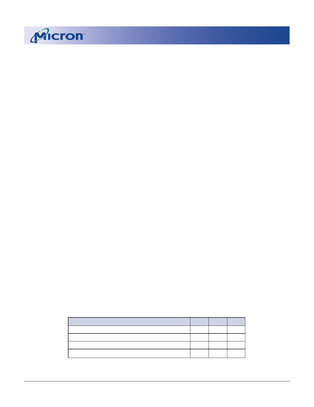
Table 5
Data Protection Combinations
DATA PROTECTION PROVIDED
All blocks locked
All blocks locked
All blocks unlocked
Boot blocks locked
VPP
≤ VPPLK
X
VPPLK
VPPLK
RP#
X
VIL
VIH
VIH
WP#
X
X
VIH
VIL
1 Meg x 16 Enhanced Boot Block Flash Memory
MT28F160A3_3.p65 – Rev. 3, Pub. 8/01
11
Micron Technology, Inc., reserves the right to change products or specifications without notice.
©2001, Micron Technology, Inc.
Share Link: 