SST27SF010-70-3C-NG Ver la hoja de datos (PDF) - Silicon Storage Technology
Número de pieza
componentes Descripción
Fabricante
SST27SF010-70-3C-NG
Silicon Storage Technology

SST27SF010-70-3C-NG Datasheet PDF : 23 Pages
| |||
512 Kbit / 1 Mbit / 2 Mbit Many-Time Programmable Flash
SST27SF512 / SST27SF010 / SST27SF020
Data Sheet
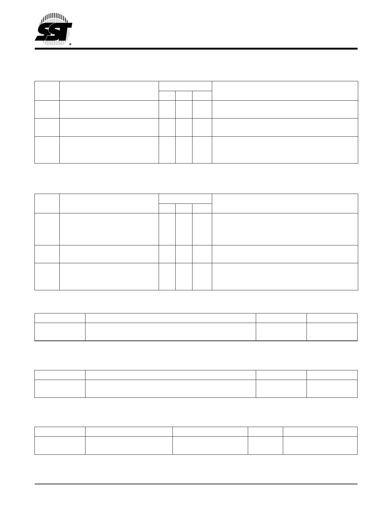
TABLE 6: PROGRAM/ERASE DC OPERATING CHARACTERISTICS FOR SST27SF512
VDD=4.5-5.5V, VPP=VPPH (TA=25°C±5°C)
Limits
Symbol Parameter
Min Max Units Test Conditions
IDD
IPP
ILI
ILO
VH
IH
VPPH
VDD Erase or Program Current
VPP Erase or Program Current
Input Leakage Current
Output Leakage Current
Supervoltage for A9
Supervoltage Current for A9
High Voltage for OE#/VPP Pin
30 mA CE#=VIL, OE#/VPP=11.4-12V, VDD=VDD Max
3 mA CE#=VIL, OE#/VPP=11.4-12V, VDD=VDD Max
1 µA VIN=GND to VDD, VDD=VDD Max
10 µA VOUT=GND to VDD, VDD=VDD Max
11.4 12 V CE#=OE#/VPP=VIL,
200 µA CE#=OE#/VPP=VIL, A9=VH Max
11.4 12 V
T6.5 1152
TABLE 7: PROGRAM/ERASE DC OPERATING CHARACTERISTICS FOR SST27SF010/020
VDD=4.5-5.5V, VPP=VPPH (TA=25°C±5°C)
Limits
Symbol Parameter
IDD
VDD Erase or Program Current
IPP
VPP Erase or Program Current
ILI
ILO
VH
IH
VPPH
Input Leakage Current
Output Leakage Current
Supervoltage for A9
Supervoltage Current for A9
High Voltage for VPP Pin
Min
11.4
11.4
Max
30
3
1
10
12
200
12
Units
mA
mA
µA
µA
V
µA
V
Test Conditions
CE#=PGM#=VIL, OE#=VIH, VPP=11.4-12V,
VDD=VDD Max
CE#=PGM#=VIL, OE#=VIH, VPP=11.4-12V,
VDD=VDD Max
VIN =GND to VDD, VDD=VDD Max
VOUT =GND to VDD, VDD=VDD Max
CE#=OE#=VIL,
CE#=OE#=VIL, A9=VH Max
T7.5 1152
TABLE 8: RECOMMENDED SYSTEM POWER-UP TIMINGS
Symbol
Parameter
Minimum
Units
TPU-READ1
TPU-WRITE1
Power-up to Read Operation
Power-up to Write Operation
100
µs
100
µs
T8.1 1152
1. This parameter is measured only for initial qualification and after a design or process change that could affect this parameter.
TABLE 9: CAPACITANCE (TA = 25°C, f=1 Mhz, other pins open)
Parameter
Description
Test Condition
Maximum
CI/O1
I/O Pin Capacitance
VI/O = 0V
12 pF
CIN1
Input Capacitance
VIN = 0V
6 pF
T9.0 1152
1. This parameter is measured only for initial qualification and after a design or process change that could affect this parameter.
TABLE 10: RELIABILITY CHARACTERISTICS
Symbol
Parameter
Minimum Specification
Units Test Method
NEND1
Endurance
1000
Cycles JEDEC Standard A117
TDR1
Data Retention
100
Years JEDEC Standard A103
T10.3 1152
1. This parameter is measured only for initial qualification and after a design or process change that could affect this parameter.
©2005 Silicon Storage Technology, Inc.
8
S71152-11-000
9/05
Share Link: