AD7951(2015) Ver la hoja de datos (PDF) - Analog Devices
NĂșmero de pieza
componentes DescripciĂłn
Fabricante
AD7951 Datasheet PDF : 32 Pages
| |||
Data Sheet
AD7951
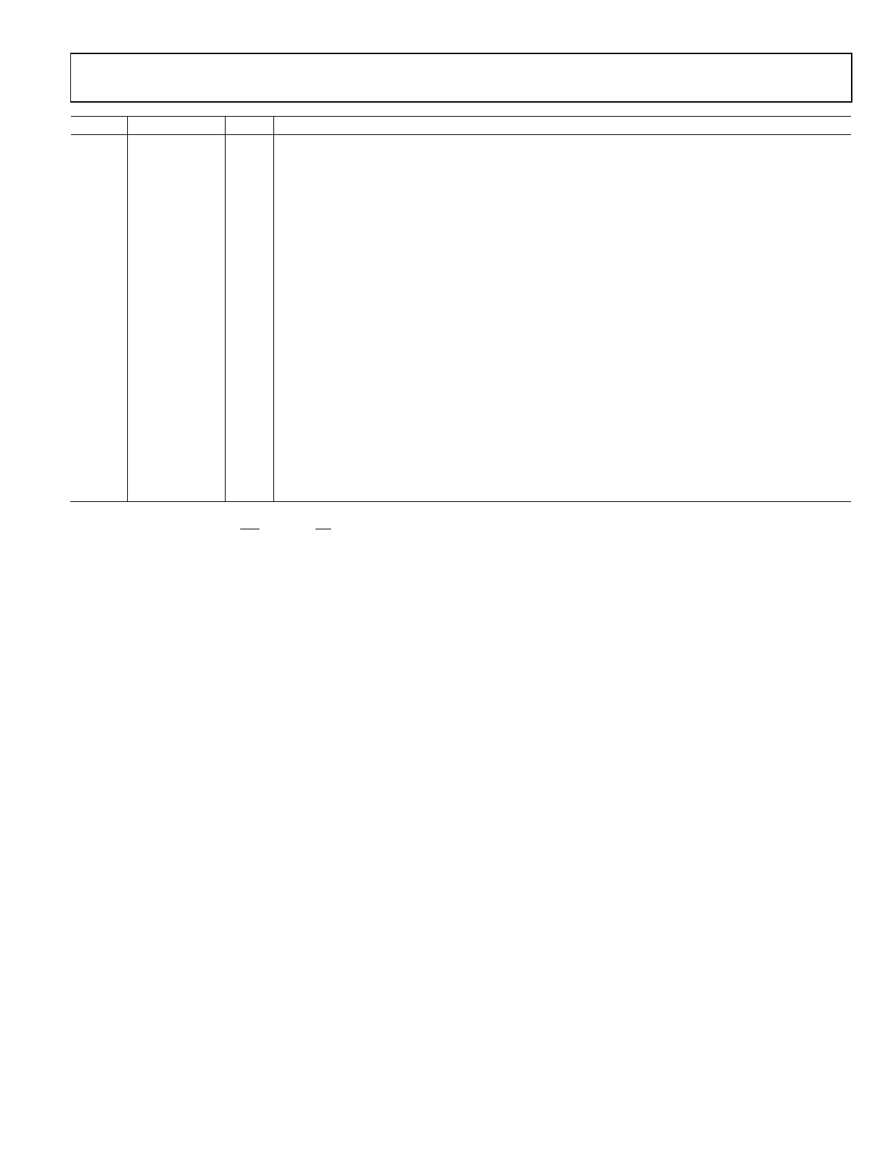
Pin No. Mnemonic
37
REF
38
REFGND
39
INâ
40
VCC
41
VEE
43
IN+
45
TEMP
46
REFBUFIN
47
PDREF
48
PDBUF
49
EPAD3
Type1
AI/O
AI
AI
P
P
AI
AO
AI
DI
DI
NC
Description
Reference Input/Output. When PDREF/PDBUF = low, the internal reference and buffer are enabled,
producing 5 V on this pin. When PDREF/PDBUF = high, the internal reference and buffer are disabled,
allowing an externally supplied voltage reference up to AVDD volts. Decoupling with at least a 22 ÎŒF is
required with or without the internal reference and buffer. See the Reference Decoupling section.
Reference Input Analog Ground. Connected to analog ground plane.
Analog Input Ground Sense. Should be connected to the analog ground plane or to a remote sense ground.
High Voltage Positive Supply. Normally +7 V to +15 V.
High Voltage Negative Supply. Normally 0 V to â15 V (0 V in unipolar ranges).
Analog Input. Referenced to INâ.
Temperature Sensor Analog Output. Enabled when the internal reference is turned on
(PDREF = PDBUF = low). See the Temperature Sensor section.
Reference Buffer Input. When using an external reference with the internal reference buffer
(PDBUF = low, PDREF = high), applying 2.5 V on this pin produces 5 V on the REF pin.
See the Voltage Reference Input section.
Internal Reference Power-Down Input.
When low, the internal reference is enabled.
When high, the internal reference is powered down, and an external reference must be used.
Internal Reference Buffer Power-Down Input.
When low, the buffer is enabled (must be low when using internal reference).
When high, the buffer is powered-down.
Exposed Pad. The exposed pad is not connected internally. It is recommended that the pad be
soldered to VEE.
1 AI = analog input; AI/O = bidirectional analog; AO = analog output; DI = digital input; DI/O = bidirectional digital; DO = digital output; P = power.
2 In serial configuration mode (SER/PAR = high, HW/SW = low), this input is programmed with the serial configuration register and this pin is a donât care. See the
Hardware Configuration section and Software Configuration section.
3 LFCSP_VQ package only.
Rev. B | Page 11 of 32
Share Link: 