CY7C1318V18 Ver la hoja de datos (PDF) - Cypress Semiconductor
Número de pieza
componentes Descripción
Fabricante
CY7C1318V18 Datasheet PDF : 24 Pages
| |||
PRELIMINARY
CY7C1316V18
CY7C1318V18
CY7C1320V18
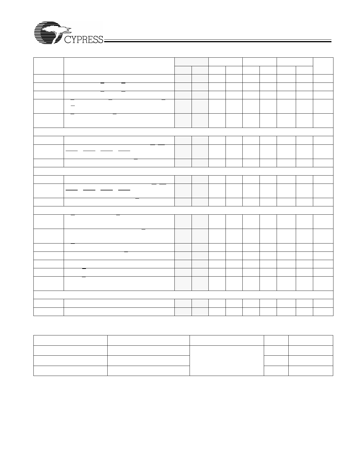
Switching Characteristics Over the Operating Range[1, 14]
300
250
200
167
Parameter
Description
Min. Max. Min. Max. Min. Max. Min. Max. Unit
tCYC
tKH
tKL
tKHKH
K Clock and C Clock Cycle Time
3.3 4.0 4.0 5.0 5.0 6.0 6.0 7.5 ns
Input Clock (K/K and C/C) HIGH
1.32 – 1.6 – 2.0 – 2.4 –
ns
Input Clock (K/K and C/C) LOW
1.32 – 1.6 – 2.0 – 2.4 –
ns
K/K Clock Rise to K/K Clock Rise and C/C to 1.49 1.82 1.8 – 2.2 – 2.7 –
ns
C/C Rise (rising edge to rising edge)
tKHCH
K/K Clock Rise to C/C Clock Rise (rising edge 0.0 1.45 0.0 1.8 0.0 2.3 0.0 2.8 ns
to rising edge)
Set-up Times
tSA
Address Set-up to K Clock Rise
0.4 – 0.5 – 0.6 – 0.7
ns
tSC
Control Set-up to Clock (K) Rise (R/W, LD, 0.4 – 0.5 – 0.6 – 0.7 –
ns
BWS0, BWS1, BWS2, BWS3)
tSD
D[x:0] Set-up to Clock (K and K) Rise
0.3 – 0.4 – 0.5 – 0.6 –
ns
Hold Times
tHA
Address Hold after Clock (K) Rise
0.4 – 0.5 – 0.6 – 0.7
ns
tHC
Control Hold after Clock (K) Rise (R/W, LD, 0.4 – 0.5 – 0.6 – 0.7 –
ns
BWS0, BWS1, BWS2, BWS3)
tHD
D[x:0] Hold after Clock (K and K) Rise
0.3 – 0.4 – 0.5 – 0.6 –
ns
Output Times
tCO
C/C Clock Rise (or K/K in single clock mode) – 0.29 – 0.35 – 0.38 – 0.40 ns
to Data Valid[14]
tDOH
Data Output Hold after Output C/C Clock Rise –0.29 – –0.35 – –0.38 – –0.40 –
ns
(Active to Active)
tCCQO
tCQOH
tCQD
tCLZ
tCHZ
C/C Clock Rise to Echo Clock Valid
– 0.27 – 0.33 – 0.36 – 0.38 ns
Echo Clock Hold after C/C Clock Rise
–0.27 – –0.27 – –0.36 – –0.38 –
ns
Echo Clock High to Data Change
–0.27 0.29 –0.33 0.35 –0.36 0.38 –0.38 0.40 ns
Clock (C) Rise to Low-Z[15, 16]
–0.29 – –0.35 – –0.38 – –0.4 –
ns
Clock (C) Rise to High-Z (Active to High-Z)[15, – 0.29 – 0.35 – 0.38 – 0.4 ns
16]
DLL Timing
tKC
tKC lock
Clock Phase Jitter
DLL Lock Time (K, C)
– 0.08 – 0.10 – 0.13
0.15 ns
1024 - 1024 – 1024 – 1024 – cycles
Capacitance[17]
Parameter
Description
Test Conditions
Max.
Unit
CIN
CCLK
CO
Input Capacitance
Clock Input Capacitance
Output Capacitance
TA = 25°C, f = 1 MHz,
VDD = 1.8V
VDDQ = 1.5V
TBD
pF
TBD
pF
TBD
pF
Notes:
14. Unless otherwise noted, test conditions assume signal transition time of 2V/ns, timing reference levels of 0.75V, VREF = 0.75V, RQ = 250Ω, VDDQ = 1.5V,
input pulse levels of 0.25V to 1.25V, and output loading of the specified IOL/IOH and load capacitance shown in (a) of AC Test Loads.
15. tCHZ, tCLZ, are specified with a load capacitance of 5 pF as in (b) of AC Test Loads. Transition is measured ± 100 mV from steady-state voltage.
16. At any given voltage and temperature tCHZ is less than tCLZ and tCHZ less than tCO.
17. Tested initially and after any design or process change that may affect these parameters.
Document #: 38-05177 Rev. *A
Page 11 of 24
Share Link: 