AD7664 Ver la hoja de datos (PDF) - Analog Devices
N├║mero de pieza
componentes Descripci├│n
Fabricante
AD7664 Datasheet PDF : 24 Pages
| |||
AD7664
CIRCUIT INFORMATION
The AD7664 is a very fast, low power, single-supply, precise
16-bit analog-to-digital converter (ADC). The AD7664 features
different modes to optimize performances according to the
applications.
In Warp Mode, the AD7664 is capable of converting 570,000
samples per second (570 kSPS).
The AD7664 provides the user with an on-chip track-and-hold,
successive-approximation ADC that does not exhibit any pipeline
or latency, making it ideal for multiple multiplexed channel
applications.
The AD7664 can be operated from a single 5 V supply and
interfaced to either 5 V or 3 V digital logic. It is housed in a
48-lead LQFP package or a 48-lead LFCSP package that
saves space and allows flexible configurations as either a
serial or parallel interface. The AD7664 is a pin-to-pin com-
patible upgrade of the AD7660.
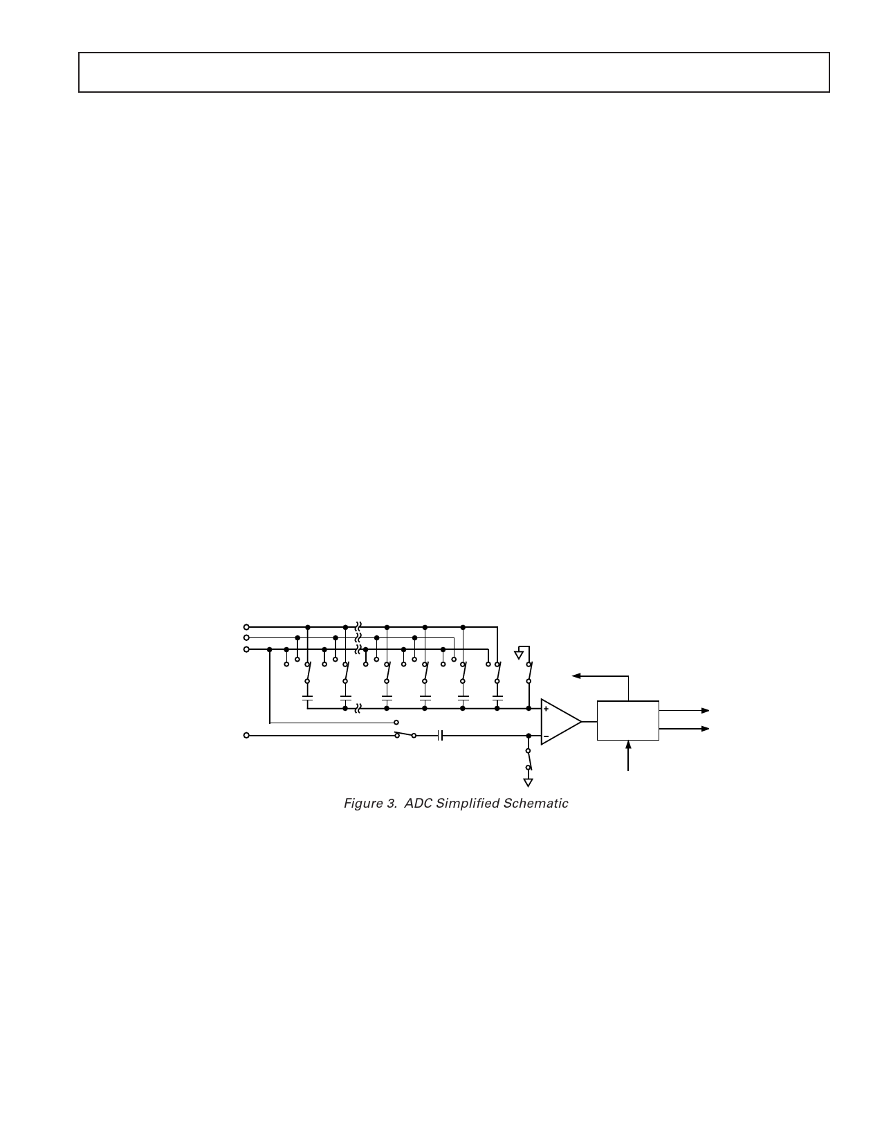
CONVERTER OPERATION
The AD7664 is a successive-approximation analog-to-digital
converter based on a charge redistribution DAC. Figure 3
shows the simplified schematic of the ADC. The capacitive
DAC consists of an array of 16 binary weighted capacitors
and an additional LSB capacitor. The comparatorΓÇÔs negative
input is connected to a dummy capacitor of the same value as
the capacitive DAC array.
During the acquisition phase, the common terminal of the array
tied to the comparatorΓÇÔs positive input is connected to AGND
via SWA. All independent switches are connected to the analog
input IN. Thus, the capacitor array is used as a sampling capacitor
and acquires the analog signal on the IN input. Similarly, the
dummy capacitor acquires the analog signal on the INGND input.
When the CNVST input goes LOW, a conversion phase is
initiated. When the conversion phase begins, SWA and SWB
are opened first. The capacitor array and the dummy capacitor
are then disconnected from the inputs and connected to the
REFGND input. Therefore, the differential voltage between IN
and INGND captured at the end of the acquisition phase is
applied to the comparator inputs, causing the comparator to
become unbalanced. By switching each element of the capacitor
array between REFGND or REF, the comparator input varies by
binary-weighted voltage steps (VREF/2, VREF/4, . . . VREF/65536).
The control logic toggles these switches, starting with the MSB
first, to bring the comparator back into a balanced condition. After
the completion of this process, the control logic generates the
ADC output code and brings BUSY output LOW.
Modes of Operation
The AD7664 features three modes of operation: Warp, Nor-
mal, and Impulse. Each of these modes is suitable for specific
applications.
The Warp Mode allows the fastest conversion rate up to 570 kSPS.
However, in this mode and this mode only, the full specified accuracy
is guaranteed only when the time between conversions does not
exceed 1 ms. If the time between two consecutive conversions is
longer than 1 ms, for instance, after power-up, the first conversion
result should be ignored. This mode makes the AD7664 ideal
for applications where both high accuracy and fast sample rate
are required.
IN
REF
REFGND
INGND
MSB
32,768C 16,384C
LSB SWA
SWITCHES
CONTROL
4C
2C
C
C
65,536C
COMP
SWB
CONTROL
LOGIC
BUSY
OUTPUT
CODE
CNVST
Figure 3. ADC Simplified Schematic
REV. E
ΓÇô11ΓÇô
Share Link: 