ST10C167-Q3 Ver la hoja de datos (PDF) - STMicroelectronics
Número de pieza
componentes Descripción
Fabricante
ST10C167-Q3 Datasheet PDF : 63 Pages
| |||
ST10R167
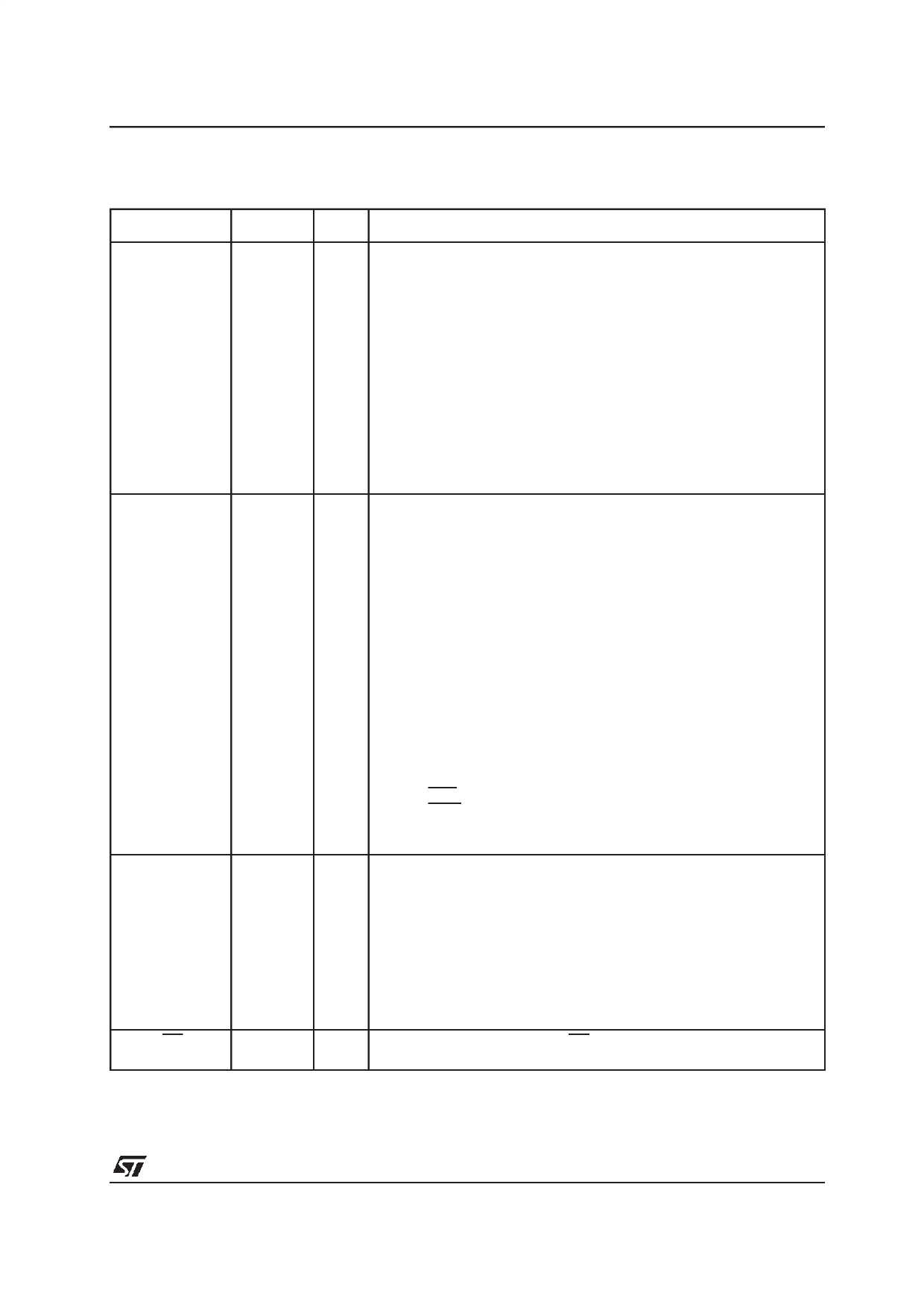
II - PIN DATA (continued)
Table 1 : Pin list (continued)
Symbol
Pin
Type
Funct ion
P2.0 - P2.7
P2.8 - P2.15
P3.0 - P3.5
P3.6 - P3.13
P3.15
P4.0 - P4.7
RD
47 - 54
57 - 64
47
...
54
57
...
64
65 - 70
73 - 80
81
65
66
67
68
69
70
73
74
75
76
77
78
79
80
81
85 - 92
85 - 89
90
91
92
95
I/O 16-bit bidirectional I/O port, bit-wise programmable for input or output via
direction bits. Programming an I/O pin as input forces the corresponding
output driver to high impedance state. Port 2 outputs can be configured as
push/pull or open drain drivers. The input threshold of Port 2 is selectable
(TTL or special).
The following Port 2 pins have alternate functions:
I/O P2.0
... ...
I/O P2.7
I/O P2.8
I EX0IN
... ...
I/O P2.15
I EX7IN
I T7IN
CC0IO
.. .
CC7IO
CC8IO
.. .
CC15IO
CAPCOM: CC0 Capture Input/Compare Output
...
CAPCOM: CC7 Capture Input/Compare Output
CAPCOM: CC8 Capture Input/Compare Output
Fast External Interrupt 0 Input
...
CAPCOM: CC15 Capture Input/Compare Output
Fast External Interrupt 7 Input
CAPCOM2 Timer T7 Count Input
I/O 15-bit (P3.14 is missing) bidirectional I/O port, bit-wise programmable for
I/O input or output via direction bits. Programming an I/O pin as input forces
I/O the corresponding output driver to high impedance state. Port 3 outputs
can be configured as push/pull or open drain drivers. The input threshold
of Port 3 is selectable (TTL or special).
The following Port 3 pins have alternate functions:
I P3.0 T0IN CAPCOM Timer T0 Count Input
O P3.1 T6OUT GPT2 Timer T6 Toggle Latch Output
I P3.2 CAPIN GPT2 Register CAPREL Capture Input
O P3.3 T3OUT GPT1 Timer T3 Toggle Latch Output
I P3.4 T3EUD GPT1 Timer T3 External Up/Down Control Input
I P3.5 T4IN GPT1 Timer T4 Input for Count/Gate/Reload/Capture
I P3.6 T3IN GPT1 Timer T3 Count/Gate Input
I P3.7 T2IN GPT1 Timer T2 Input for Count/Gate/Reload/Capture
I/O P3.8 MRST SSC Master-Receive/Slave-Transmit I/O
I/O P3.9 MTSR SSC Master-Transmit/Slave-Receive O/I
I/O P3.10 TxD0 ASC0 Clock/Data Output (Asynchronous/Synchronous)
O P3.11 RxD0 ASC0 Data Input (Asyn.) or I/O (Synchronous)
O P3.12 BHE External Memory High Byte Enable Signal,
WRH External Memory High Byte Write Strobe
I/O P3.13 SCLK SSC Master Clock Output/Slave Clock Input
O P3.15 CLKOUT System Clock Output (=CPU Clock)
I/O 8-bit bidirectional I/O port, bit-wise programmable for input or output via
direction bits. Programming an I/O pin as input forces the corresponding
output driver to high impedance state. For external bus configuration,
Port 4 can be used to output the segment address lines:
O P4.0 - P4.4 A16 - A20 Least Significant Segment Address Line
O P4.5
A21
Segment Address Line
I
CAN_RxD CAN Receive Data Input
O P4.6
A22
Segment Address Line,
O
CAN_TxD CAN Transmit Data Output
O P4.7
A23
Most Significant Segment Address Line
O External Memory Read Strobe. RD is activated for every external instruc-
tion or data read access.
7/63
Share Link: 