PCF1252 Ver la hoja de datos (PDF) - Philips Electronics
Número de pieza
componentes Descripción
Fabricante
PCF1252 Datasheet PDF : 16 Pages
| |||
Philips Semiconductors
Threshold detector and reset generator
Product specification
PCF1252-X family
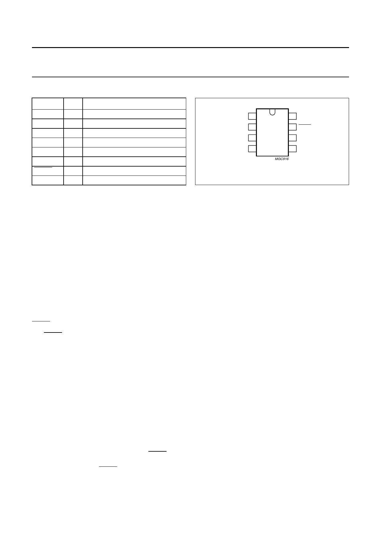
PINNING
SYMBOL PIN
DESCRIPTION
CT
1 connection for the external capacitor
SELECT 2 select polarity or external reset input
COMIN
3 comparator input
VSS
4 ground (0 V)
COMOUT 5 comparator output
RESET
6 reset output
POWF
7 power failure signal output
VDD
8 supply voltage
handbook, halfpage
CT 1
8 VDD
SELECT 2
7 POWF
PCF1252-X
COMIN 3
6 RESET
VSS 4
5 COMOUT
MGC916
Fig.2 Pinning diagram.
FUNCTIONAL DESCRIPTION (see Fig.1)
The PCF1252-X contains:
• A precise factory-programmed voltage reference
• Two comparators
• A delay circuit.
The PCF1252-X family is comprised of 10 versions with
different factory-programmed voltage trip-points (VTRIP),
see Chapter “Characteristics”.
Supply
The supply voltage (VDD) is internally divided before being
compared, via comparator 1, with the internal reference
voltage.
POWF (see Fig.3)
The POWF output is:
• LOW, if VDD is below VTRIP
• HIGH, if VDD is above VTRIP.
Power-on reset (SELECT = LOW)
As VDD rises past VTRIP, a positive reset pulse is generated
at RESET. The duration of the reset pulse (tR) is
determined by the value of the external capacitor (CCT;
maximum 1 µF, see Fig.8) connected to CT. With no
external capacitor connected, CCT assumes a minimum
value of 100 pF. If SELECT is HIGH, the reset pulse is
inverted.
Voltage trip-point
By selecting the voltage trip-point slightly higher than the
minimum operating voltage of the
microcontroller/microprocessor, there is sufficient time for
data storage before the power actually fails.
In order to prevent oscillations around the voltage
trip-point, a small hysteresis has been included, resulting
in a power-on switching point that is higher than the
voltage trip-point (minimum of 15 mV). The voltage
trip-point refers to the value at which power-off is signalled.
COMIN
Input to the second comparator (comparator 2).
When used in conjunction with an external voltage divider,
this allows a second point in the system to be monitored.
This input has no built-in hysteresis. When not in use
connect to VDD. COMOUT will be LOW or HIGH
depending on the voltage at COMIN:
• COMOUT = HIGH, if voltage at COMIN is above the
switch point VSP (typically 1.30 V).
• COMOUT = LOW, if voltage at COMIN is below the
switch point VSP (typically 1.30 V).
Power failure
During a power-off condition (VDD < VTRIP), POWF goes
LOW. After a time delay (tS), also determined by CCT,
RESET goes HIGH. Any POWF assertion (VDD < VTRIP)
will result in a subsequent RESET pulse.
1998 Apr 16
3
Share Link: 