NX25P10 Ver la hoja de datos (PDF) - Unspecified
Número de pieza
componentes Descripción
Fabricante
NX25P10 Datasheet PDF : 28 Pages
| |||
1M / 2M / 4M-BIT SERIAL FLASH MEMORY with 40MHz SPI
NX25P10, NX25P20 AND NX25P40
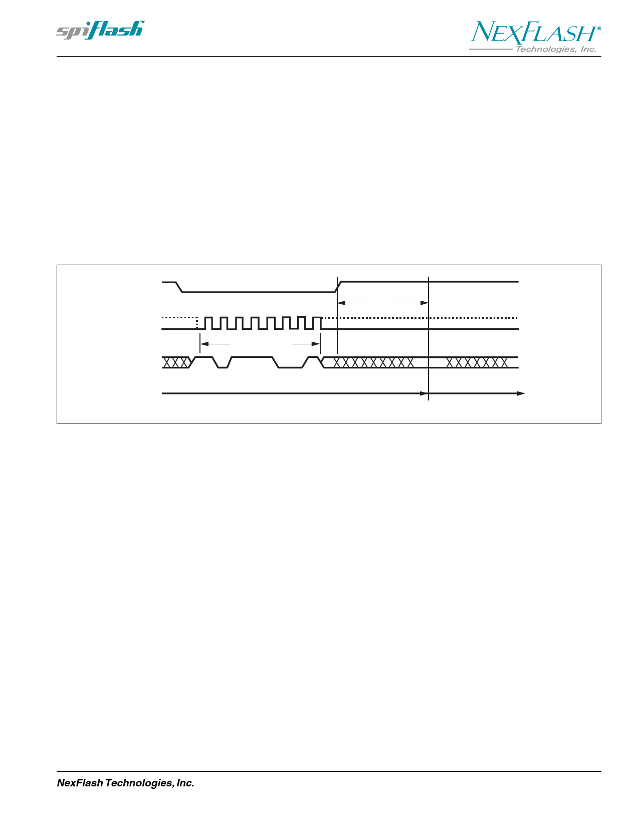
Power-down (B9h)
Although the standby current during normal operation is
relatively low, standby current can be further reduced with
the Power-down instruction. The lower power consumption
makes the Power-down instruction especially useful for
battery powered applications (See ICC1 and ICC2 in AC
Characteristics). The instruction is initiated by driving the
CS pin low and shifting the instruction code “B9h” as shown
in figure 13.
The CS pin must be driven high after the eighth bit has been
latched. If this is not done the Power-down instruction will
not be executed. After CS is driven high, the power-down
1 state will entered within the time duration of tDP (See AC
Characteristics). While in the power-down state only the
Release from Power-down / Device ID instruction, which
restores the device to normal operation, will be recognized.
2 All other instructions are ignored. This includes the Read
Status Register instruction, which is always available
during normal operation. Ignoring all but one instruction
makes the Power Down state a useful condition for securing
3 maximum write protection. The device always powers-up in
the normal operation with the standby current of ICC1.
CS
4
tDP
Mode 3
01 2 3 456 7
CLK Mode 0
5
Instruction (B9h)
DI
High Impedance
DO
6
Stand-by Current
Power-down Current
Figure 13. Deep Power-down Instruction Sequence Diagram
7
8
9
10
11
12
NexFlash Technologies, Inc.
19
PRELIMINARY MKP-0009 Rev 6 NXSF040I-0405
04/04/05 ©
Share Link: 