MPC9600 Ver la hoja de datos (PDF) - Motorola => Freescale
Número de pieza
componentes Descripción
Fabricante
MPC9600 Datasheet PDF : 16 Pages
| |||
Freescale Semiconductor, Inc.
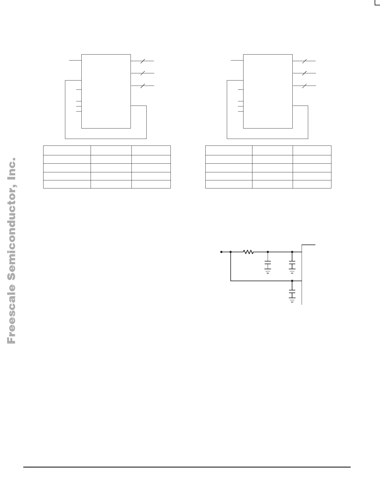
Figure 3. Configuration for 125 MHz clocks
fref = 20.833 MHz
CCLK
QA0–6
FB_IN
1 FSEL_FB
QB0–6
QC0–6
0 FSELA
0 FSELB
QFB
0 FSELC
MPC9600
20.833 MHz (Feedback)
125 MHz
7
125 MHz
7
125 MHz
7
Frequency range
Input
QA outputs
QB outputs
QC outputs
Min
16.67 MHz
100 MHz
100 MHz
100 MHz
Max
33.33 MHz
200 MHz
200 MHz
200 MHz
Figure 4. Configuration for 133.3/66.67 MHz clocks
fref = 33.33 MHz
CCLK
QA0–6
FB_IN
0 FSEL_FB
QB0–6
QC0–6
0 FSELA
1 FSELB
QFB
1 FSELC
MPC9600
33.33 MHz (Feedback)
133.3 MHz
7
66.67 MHz
7
66.67 MHz
7
Frequency range
Input
QA outputs
QB outputs
QC outputs
Min
25 MHz
100 MHz
100 MHz
100 MHz
Max
50 MHz
200 MHz
200 MHz
200 MHz
Power Supply Filtering
The MPC9600 is a mixed analog/digital product. Its analog
circuitry is naturally susceptible to random noise, especially if
this noise is seen on the power supply pins. Random noise
on the VCCA (PLL) power supply impacts the device
characteristics, for instance I/O jitter. The MPC9600 provides
separate power supplies for the output buffers (VCC) and the
phase-locked loop (VCCA) of the device.The purpose of this
design technique is to isolate the high switching noise digital
outputs from the relatively sensitive internal analog
phase-locked loop. In a digital system environment where it
is more difficult to minimize noise on the power supplies a
second level of isolation may be required. The simple but
effective form of isolation is a power supply filter on the VCCA
pin for the MPC9600. Figure 5. illustrates a typical power
supply filter scheme. The MPC9600 frequency and phase
stability is most susceptible to noise with spectral content in
the 100kHz to 20MHz range. Therefore the filter should be
designed to target this range. The key parameter that needs
to be met in the final filter design is the DC voltage drop
across the series filter resistor RF. From the data sheet the
ICCA current (the current sourced through the VCCA pin) is
typically 3 mA (5 mA maximum), assuming that a minimum of
2.325 V (VCC=3.3 V or VCC=2.5 V) must be maintained on
W the VCCA pin. The resistor RF shown in Figure 5. “VCCA
Power Supply Filter” must have a resistance of 9-10
(VCC=2.5 V) to meet the voltage drop criteria.
The minimum values for RF and the filter capacitor CF are
defined by the required filter characteristics: the RC filter
should provide an attenuation greater than 40 dB for noise
whose spectral content is above 100 kHz. In the example RC
filter shown in Figure 5. “VCCA Power Supply Filter”, the filter
cut-off frequency is around 3-5 kHz and the noise attenuation
at 100 kHz is better than 42 dB.
RF = 9–10 Ω for VCC = 2.5 V or VCC = 3.3 V
CF = 22 µF for VCC = 2.5 V or VCC = 3.3 V
RF
VCC
VCCA
CF
10 nF
MPC9600
VCC
33...100 nF
Figure 5. VCCA Power Supply Filter
As the noise frequency crosses the series resonant point
of an individual capacitor its overall impedance begins to look
inductive and thus increases with increasing frequency. The
parallel capacitor combination shown ensures that a low
impedance path to ground exists for frequencies well above
the bandwidth of the PLL. Although the MPC9600 has
several design features to minimize the susceptibility to
power supply noise (isolated power and grounds and fully
differential PLL) there still may be applications in which
overall performance is being degraded due to system power
supply noise. The power supply filter schemes discussed in
this section should be adequate to eliminate power supply
noise related problems in most designs.
MOTOROLA
For More Informa8tion On This Product,
Go to: www.freescale.com
TIMING SOLUTIONS
Share Link: 